Wafer inspection apparatus

a technology of inspection apparatus and wafer, which is applied in the direction of material analysis, semiconductor/solid-state device testing/measurement, instruments, etc., can solve the problems of poor imaging accuracy, inability to observe the front side bevel sa, the apex ss, and the back side bevel sb to be observed simultaneously in a clear condition, so as to improve the imaging accuracy and improve the detection accuracy

Inactive Publication Date: 2006-12-12
COVALENT MATERIALS CORP +1
View PDF25 Cites 27 Cited by
  • Summary
  • Abstract
  • Description
  • Claims
  • Application Information

AI Technical Summary

Benefits of technology

[0009]An object of the present invention is to provide a wafer inspection apparatus, which can improve accuracy of imaging and improve accuracy of detection of defects, by clearly imaging a plurality of different parts in a thickness direction, even if a circumferential edge of a wafer is beveled so as to be inclined relative to an apex.

Problems solved by technology

Therefore, accuracy of detecting defects is bad.
As a result, accuracy of imaging becomes bad.
Further, there was a problem such that the apex SS, the front side bevel SA, and the back side bevel SB could not be observed simultaneously in a clear condition.

Method used


Image

  • Wafer inspection apparatus
  • Wafer inspection apparatus
  • Wafer inspection apparatus

Examples


Embodiment Construction

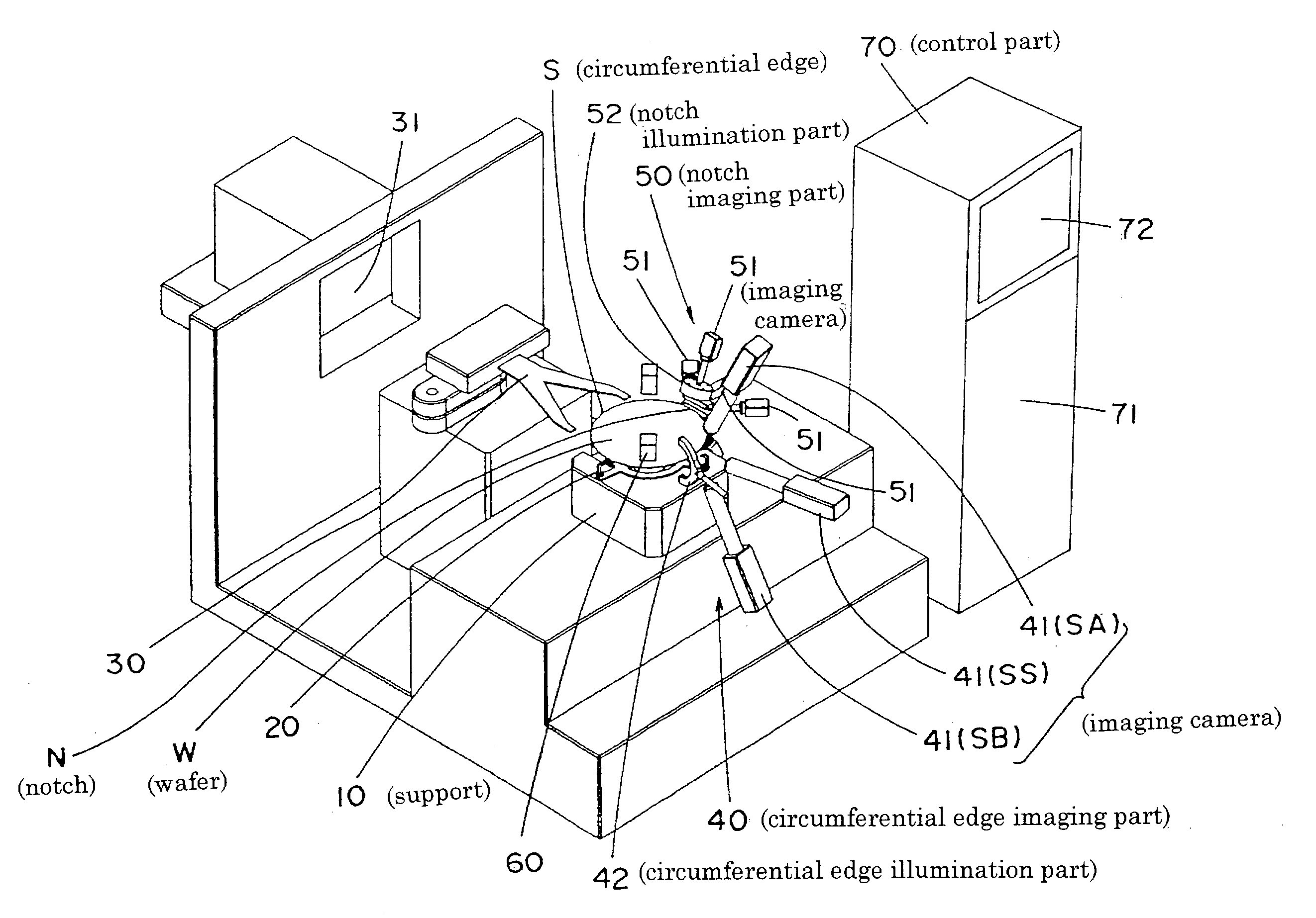
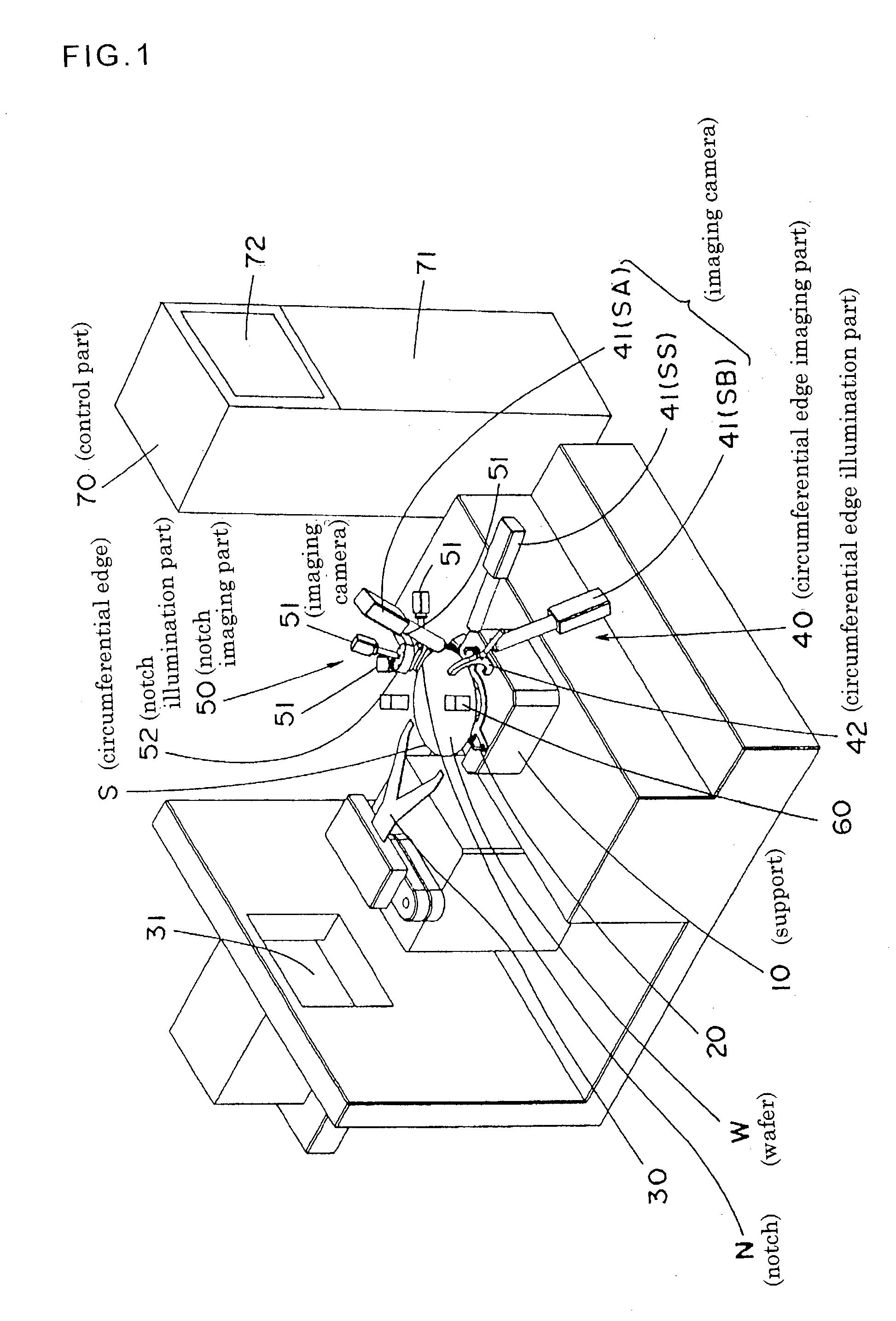
[0075]In a wafer inspection apparatus shown in FIGS. 1˜11, a wafer W to be inspected is formed of a disk.

[0076]Particularly, as shown in FIGS. 12 and 13, a circumferential edge S of the wafer W has an apex SS, a front side bevel SA, and a back side bevel SB. The apex SS is substantially at right angles to a surface of the wafer W. The front side bevel SA and the back side bevel SB are inclined relative to the apex SS. Upper and lower parts of the circumferential edge S are beveled so as to incline the front side bevel SA and the back side bevel SB.

[0077]Further, at a predetermined position in a peripheral direction of the circumferential edge S of the wafer W, a notch (namely a notch N that includes a bottom Nt, one side part Na and the other side part Nb and that is cutout in a substantially U-shape) is formed.

[0078]On the notch N, the apex SS, the front side bevel SA, and the back side bevel SB are also formed. The apex SS is substantially at right angles to a surface of the wafer...


PUM

PropertyMeasurementUnit
diameteraaaaaaaaaa
anglesaaaaaaaaaa
anglesaaaaaaaaaa

Abstract

A wafer inspection apparatus has a supporting means (10) for rotatably supporting a wafer (W) formed of a disk, a circumferential edge imaging means (40) for imaging a circumferential edge (S) of the wafer (W) that is supported by the supporting means for rotation, a notch imaging means (50) for imaging a notch (N), a notch illumination part (52) for illuminating the notch (N), and a control means (70) for processing image data imaged by the circumferential edge imaging means (40) and the notch imaging means (50). The circumferential edge imaging means (40) has a plurality of imaging cameras (41) for imaging a plurality of different parts in a thickness direction of the circumferential edge of the wafer (W). The different parts of the circumferential edge (S) of the wafer (W) include an apex at right angles to a surface of the wafer (W) and a front side bevel and a back side bevel inclined relative to the apex. The notch imaging means (50) for the wafer (W) having the notch (N) has a plurality of imaging cameras (51) for imaging different parts in the thickness direction of the notch (N).

Description

TECHNICAL FIELD[0001]The present invention relates to a wafer inspection apparatus for imaging a circumferential edge of a wafer formed of a disk and inspecting the wafer based on image data without destruction.RELATED ART[0002]A prior wafer inspection apparatus is described, for example, in Japanese Patent Unexamined Publication No.8-136462.[0003]This wafer inspection apparatus includes, as shown in FIG. 34, a support 1, an imaging camera 2, and a monitor (not shown). The support 1 rotatably supports a wafer W formed of a disk. The imaging camera 2 continuously images a circumferential edge S of the wafer W that is supported by the support 1 and rotated. The monitor, such as CRT, displays an image obtained by the imaging camera 2.[0004]The imaging camera 2 is provided movably all around the wafer W and rotatably in a thickness direction of the wafer W. By this movement and rotation, an operation direction and a distance of the imaging camera are adjusted.[0005]The circumferential e...

Claims


Application Information

Patent Timeline
Patent Type & Authority Patents(United States)
IPC IPC(8): G06K9/00G01N21/00H01L21/66G01N21/95
CPCG01N21/9503H01L22/00
Inventor HAYASHI, YOSHINORINARAIDATE, HIROYUKIYUDA, HIROAKITANABE, ATSUSHIISOGAI, HIROMICHIIZUNOME, KOJI
Owner COVALENT MATERIALS CORP
Why Eureka
Try Eureka