MRAM arrays and methods for writing and reading magnetic memory devices
a magnetic memory device and array technology, applied in the field of magnetic memory arrays and circuits, can solve the problems of poor cell density of fig. 1, insufficient cell density, and insufficient mram density for today's market demands
- Summary
- Abstract
- Description
- Claims
- Application Information
AI Technical Summary
Problems solved by technology
Method used
Image

Examples
first embodiment
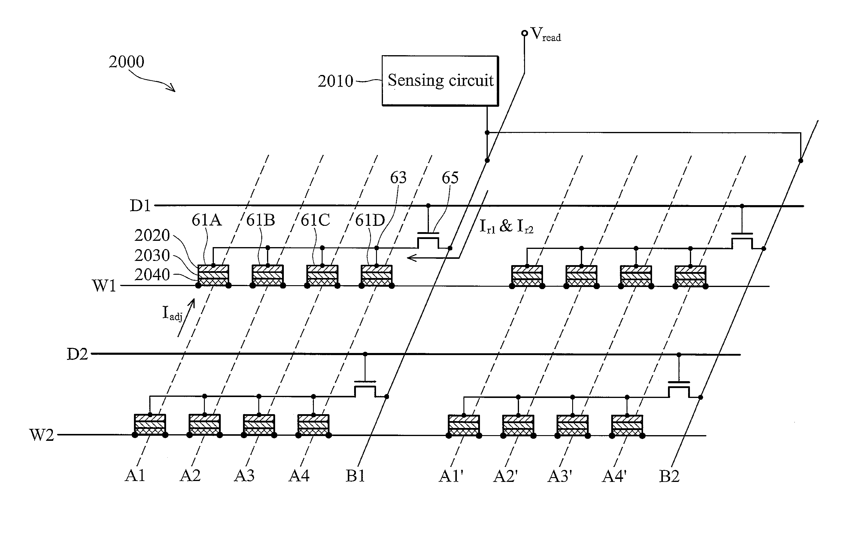
[0098]FIG. 20 illustrates a schematic circuit diagram illustrative of one memory array 2000 of MTJ memory devices according to the invention. The MRAM array 2000 comprises data lines D1 and D2, bit lines B1 and B2, and word lines W1 and W2. MTJ memory devices 61A, 61B, 61C, and 61D are connected in parallel between node 63 and word line W1. Each MTJ memory device comprises a free ferromagnetic layer 2020, a pinned ferromagnetic layer 2040, and an insulating tunneling barrier 2030 located between the pinned ferromagnetic layer 2040 and the free ferromagnetic layer 2020. The free ferromagnetic layer 2020 has a freely changeable magnetic moment, the pinned ferromagnetic layer 2040 has a fixed magnetic moment, and the insulating tunneling barrier 2030 is a very thin insulation layer.
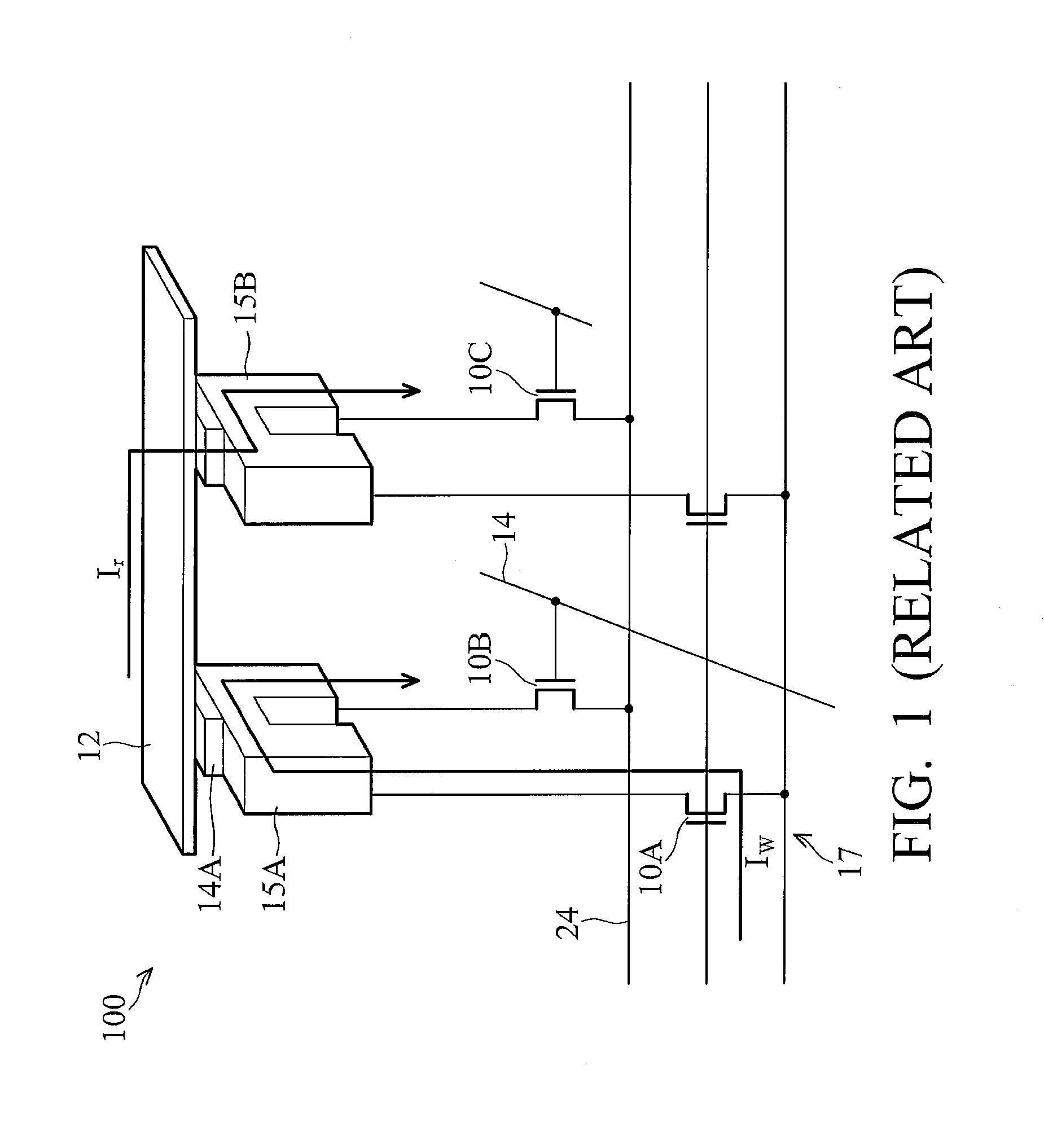
[0099]The NMOS transistor of switch 65, for example, is connected between bit line B1 and the node 63, and controlled by a selection signal provided by data line D1. In the exemplary embodiment of FIG. 20, t...
second embodiment
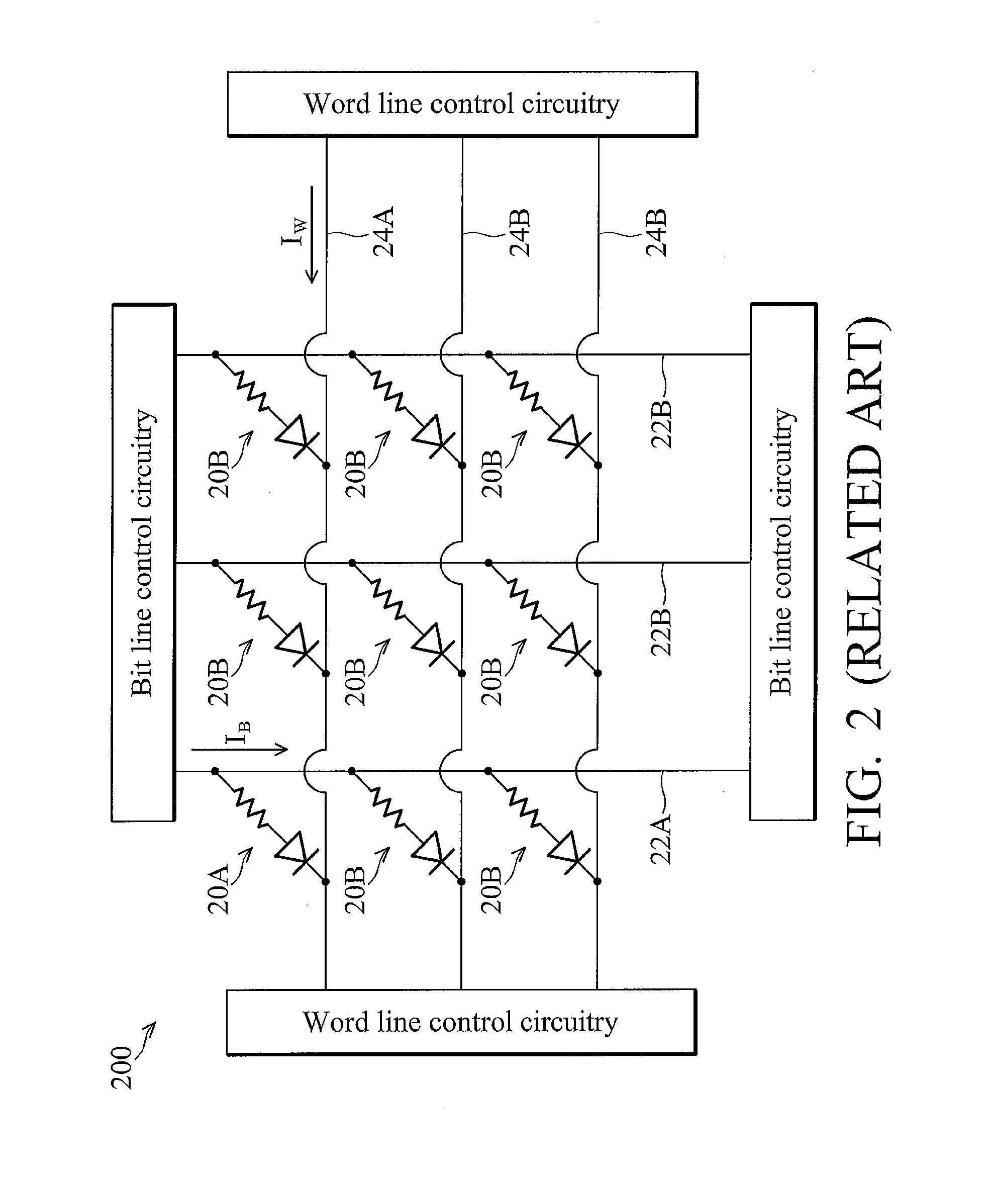
[0107]FIG. 24 is a schematic circuit diagram illustrative of one memory array circuit 2400 of MTJ memory devices according to a single switch arrangement disclosed herein. The MRAM array circuit 2400 comprises data lines D1 and D2, bit lines B1 and B2, and word lines W1 and W2. MTJ memory devices 71A, 71B, 71C, and 71D are connected in parallel between node 73 and bit line B1. Each MTJ memory device comprises a free ferromagnetic barrier 2420, a pinned ferromagnetic barrier 2440, and an insulating tunneling barrier 2430 located between the pinned ferromagnetic barrier 2440 and the free ferromagnetic barrier 2420. The free ferromagnetic barrier 2420 has a freely changeable magnetic moment, the pinned ferromagnetic barrier 2440 has a fixed magnetic moment, and the insulating tunneling barrier 2430 is a very thin insulation layer.
[0108]Switch 2450, an NMOS transistor in this example, is connected between word line W1 and the node 73, and is controlled by a selection signal provided by ...
third embodiment
[0114]FIG. 25 is a schematic circuit diagram illustrative of one memory array 2500 of MTJ memory devices according to the single switch arrangement disclosed herein. The MRAM array circuit 2500 comprises data lines D1 and D2, bit lines B1 and B2, and word lines W1 and W2. MTJ memory devices 81A, and 81B are connected in parallel between nodes 82 and 83, MTJ memory devices 81C, and 81D are connected in parallel between node 82 and bit line B1. Here, the MTJ memory devices connected in parallel comprise a MTJ memory device group, and the MTJ memory device groups are connected in serial. For example, MTJ memory devices 81A and 81B comprise a first MTJ memory device group, MTJ memory devices 81C and 81D comprise a second MTJ memory device group, and the first and second MTJ memory device groups are connected in serial.
[0115]In another embodiment, MTJ memory devices 81A and 81B are connected serially and comprise a first MTJ memory device group; MTJ memory devices 81C and 81D are connect...
PUM
 Abstract
Description
Claims
Application Information
 - R&D
- Intellectual Property
- Life Sciences
- Materials
- Tech Scout
- Unparalleled Data Quality
- Higher Quality Content
- 60% Fewer Hallucinations
Browse by: Latest US Patents, China's latest patents, Technical Efficacy Thesaurus, Application Domain, Technology Topic, Popular Technical Reports.
© 2025 PatSnap. All rights reserved.Legal|Privacy policy|Modern Slavery Act Transparency Statement|Sitemap|About US| Contact US: help@patsnap.com