Non-volatile semiconductor memory device

a semiconductor memory and non-volatile technology, applied in static storage, digital storage, instruments, etc., can solve the problems of disadvantageously taking a long time to rewrite data, affecting the performance of data rewriting, and affecting the accuracy of data rewriting

Active Publication Date: 2007-01-09
CETUS TECH INC
View PDF10 Cites 5 Cited by
  • Summary
  • Abstract
  • Description
  • Claims
  • Application Information

AI Technical Summary

Benefits of technology

[0033]Therefore, an object of the present invention is to provide a non-volatile semiconductor memory device in which data can be rewritten quickly and an error is unlikely to occur in reading, and a production method thereof.

Problems solved by technology

When the difference between the read voltage and the reference voltage becomes small, an error occurs in reading the data.
Therefore, in the non-volatile semiconductor memory device of FIG. 10, the voltage difference used for the data determination during a read operation is larger than that of the conventional non-volatile semiconductor memory device, so that an error is unlikely to occur in reading data.
Therefore, even when the amount of electrons to be injected into the floating gates 1006 and 1010 is smaller than that of the conventional non-volatile semiconductor device, an error occurs with a lower possibility in reading data.
Therefore, in the non-volatile semiconductor memory device of FIG. 10, it disadvantageously takes a long time to rewrite data.
As a result, the differential amplifier can no longer determine data stored in the memory cell when reading out the data.
Therefore, it disadvantageously takes a long time to rewrite data in the non-volatile semiconductor memory device of FIG. 10.

Method used


Image

  • Non-volatile semiconductor memory device
  • Non-volatile semiconductor memory device
  • Non-volatile semiconductor memory device

Examples


first embodiment

[0056](First embodiment)

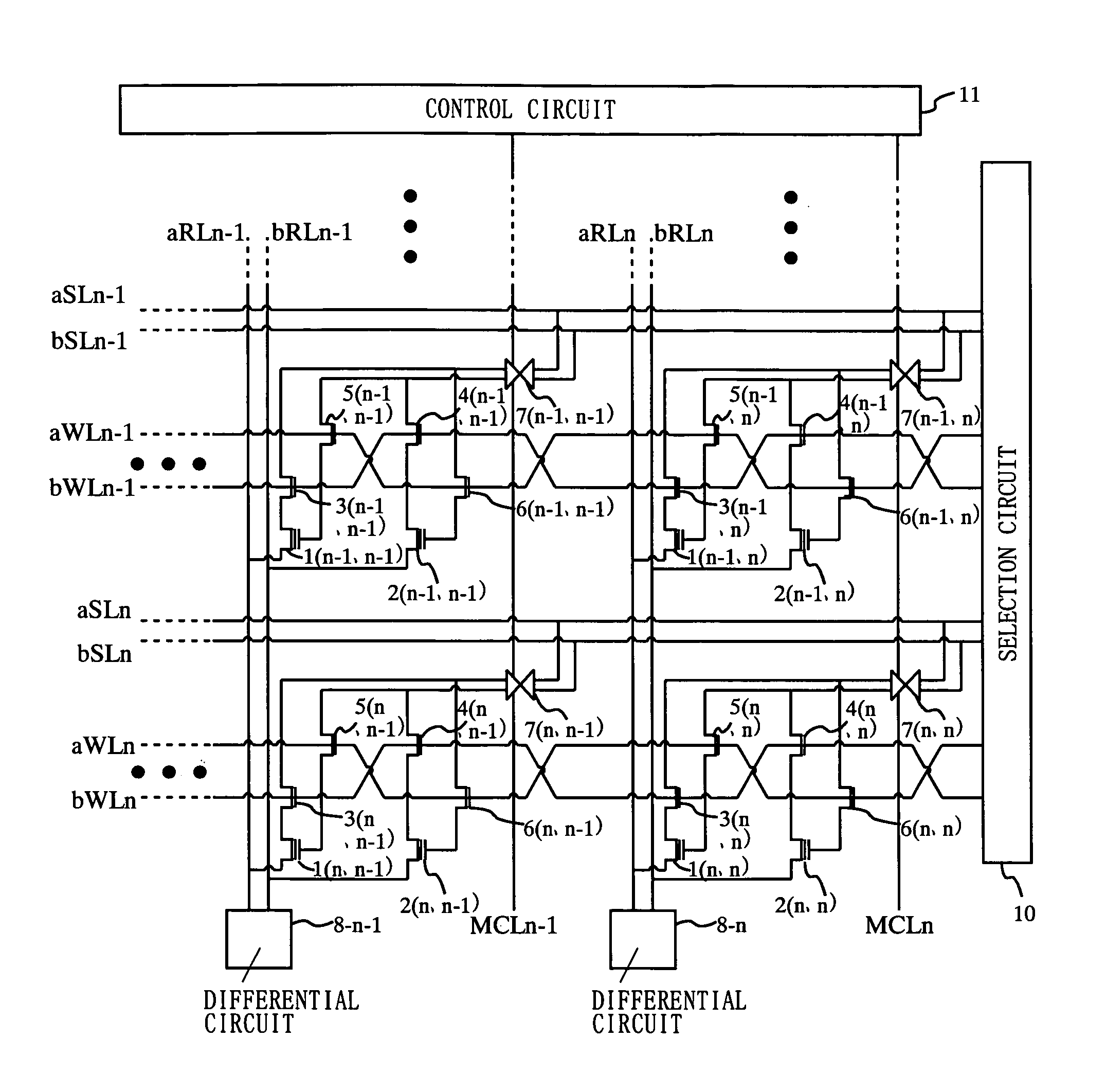
[0057]Hereinafter, a non-volatile semiconductor memory device according to a first embodiment of the present invention will be described with reference to the accompanying drawings. FIG. 1 is a diagram illustrating a structure of a non-volatile semiconductor memory device according to the first embodiment of the present invention. In the non-volatile semiconductor memory device of FIG. 1, memory cells are arranged in a matrix of n×n (n is a natural number). Note that FIG. 1 illustrates an extracted portion of the non-volatile semiconductor memory device.

[0058]The non-volatile semiconductor memory device of FIG. 1 comprises memory cells, source lines aSL1 to aSLn, source lines bSL1 to bSLn, word lines aWL1 to aWLn, word lines bWL1 to bWLn, lead lines aRL1 to aRLn, lead lines bRL1 to bRLn, multiplexer control lines MCL1 to MCLn, differential circuits 8-1 to 8-n, a selection circuit 10, and a control circuit 11. The number of the memory cells is n×n. Each memory...

second embodiment

[0088](Second embodiment)

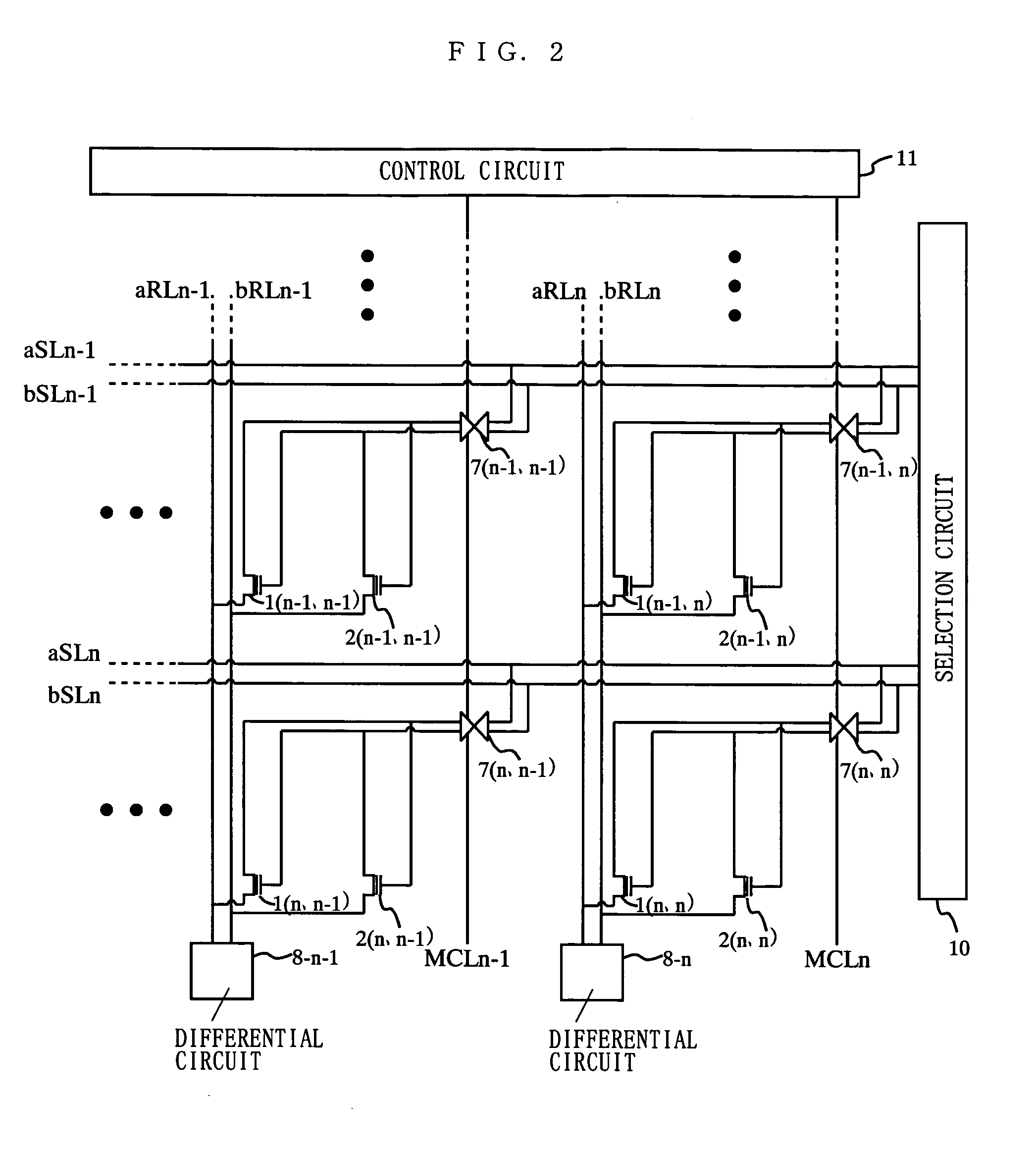
[0089]Hereinafter, a non-volatile semiconductor memory device according to a second embodiment of the present invention will be described with reference to the accompanying drawings. FIG. 2 is a diagram illustrating a structure of the non-volatile semiconductor memory device of the second embodiment of the present invention. In the non-volatile semiconductor memory device of FIG. 2, memory cells are arranged in a matrix of n×n (n is a natural number). FIG. 2 illustrates an extracted portion of the non-volatile semiconductor memory device.

[0090]The non-volatile semiconductor memory device of FIG. 2 comprises memory cells, source lines aSL1 to aSLn, source lines bSL1 to bSLn, lead lines aRL1 to aRLn, lead lines bRL1 to bRLn, multiplexer control lines MCL1 to MCLn, differential circuits 8-1 to 8-n, a selection circuit 10, and a control circuit 11. The number of the memory cells is n×n, each of which comprises a memory transistor 1, a memory transistor 2 and a m...

third embodiment

[0114](Third embodiment)

[0115]Hereinafter, a non-volatile semiconductor memory device according to a third embodiment of the present invention will be described with reference to the accompanying drawings. FIG. 3 is a diagram illustrating a structure of the non-volatile semiconductor memory device of the third embodiment of the present invention. In the non-volatile semiconductor memory device of FIG. 3, memory cells are arranged in a matrix of n×n (n is a natural number). FIG. 3 illustrates an extracted portion of the non-volatile semiconductor memory device.

[0116]The non-volatile semiconductor memory device of FIG. 3 comprises memory cells, source lines aSL1 to aSLn and bSL1 to bSLn, word lines aWL1 to aWLn, bit lines BL1 to BLn, lead lines aRL1 to aRLn and bRL1 to bRLn, multiplexer control lines MCL1 to MCLn, a differential circuit 8, a selection circuit 10, and a control circuit 11. The number of the memory cells is n×n, each of which comprises a memory transistor 1, a memory tr...


PUM


Abstract

A switch section connects a first wire line aSL to the gate of a first memory transistor 1 and the source of a second memory transistor 2 and a second wire line bSL to the source of the first memory transistor 1 and the gate of the second memory transistor 2 when first type data is to be written into a memory cell; and connects the first wire line aSL to the source of the first memory transistor 1 and the gate of the second memory transistor 2 and the second wire line bSL to the gate of the first memory transistor 1 and the source of the second memory transistor 2 when second type data is to be written into a memory cell.

Description

BACKGROUND OF THE INVENTION[0001]1. Field of the Invention[0002]The present invention relates to a non-volatile semiconductor memory device, and more particularly, a non-volatile semiconductor memory device in which a plurality of memory cells for storing data are arranged in a matrix.[0003]2. Description of the Background Art[0004]Electrically rewritable non-volatile semiconductor memory devices (hereinafter referred to as “non-volatile semiconductor memory devices”) have a property such that data is not lost when the device is powered off. Conventional non-volatile semiconductor memory devices have a structure which is described in, for example, “Furasshu Memori Gijyutsu Hando Bukku [Flash Memory Technical Handbook]” (Fujio Masoka, et al., 1993, Science Forum, p. 37). Hereinafter, conventional non-volatile semiconductor memory devices will be described.[0005]In a conventional non-volatile semiconductor memory device, a rewrite operation is achieved by injection or ejection of elec...

Claims


Application Information

Patent Timeline
Patent Type & Authority Patents(United States)
IPC IPC(8): G11C11/34G11C16/04G11C14/00
CPCG11C16/0441G11C14/00
Inventor KATO, JUNICHINAKAYAMA, MASAYOSHIOZEKI, TAKAOMIYOSHI, ASAKOHATAKEYAMA, SHINICHI
Owner CETUS TECH INC
Why Eureka
Try Eureka