Non-volatile memory and method of manufacturing the same

a technology of non-volatile memory and manufacturing method, which is applied in the direction of electrical equipment, semiconductor devices, instruments, etc., can solve the problems of serious impairment of the insulation characteristic of the tunnel oxide film at the active layer side, degradation of the etc., and achieve enhanced electric charge holding characteristic, reduced leakage current from the floating gate to the active layer, and more thin

Inactive Publication Date: 2009-06-23
SEMICON ENERGY LAB CO LTD
View PDF21 Cites 8 Cited by
  • Summary
  • Abstract
  • Description
  • Claims
  • Application Information

AI Technical Summary

Benefits of technology

[0032]The present invention having the above structures is capable of avoiding thinning of a tunnel oxide film as well as electric field concentration at semiconductor side end corners. Therefore the present invention can provide a non-volatile memory in which a leak current from a floating gate to an active layer is reduced and a manufacturing method thereof. The invention can also provide a non-volatile memory with an enhanced electric charge holding characteristic and a manufacturing method thereof. Furthermore, the present invention can provide a non-volatile memory in which an insulating film is made more thin while keeping the electric charge holding characteristic to achieve lower voltage operation, quicker rewriting, and less power consumption, and a manufacturing method thereof.

Problems solved by technology

However, in a normal TFT manufacturing process, an active layer formed by a semiconductor thin film etching process drops off sharply along the sides like a cliff.
As described above, the insulating characteristic of a tunnel oxide film is seriously impaired at active layer side ends when a memory TFT is fabricated through the active layer formation process and the thermal oxidization process for obtaining a quality tunnel oxide film in a normal TFT manufacturing process.
With the semiconductor active layer side end corners pointed, another problem is raised, in which the electric field created by electric charges that are accumulated in the floating gate concentrates around the active layer side end corners even when no voltage is applied to a control gate.
These problems mean an increase in leak current flowing from the floating gate through the active layer side end corners to the active layer in the memory TFT, leading to degradation in electric charge holding characteristic.
These problems caused by thermal oxidization of the active layer side ends similarly occur in the case where formation of the oxide film by CVD apparatus or the like precedes thermal oxidization.

Method used


Image

  • Non-volatile memory and method of manufacturing the same
  • Non-volatile memory and method of manufacturing the same
  • Non-volatile memory and method of manufacturing the same

Examples


embodiment 1

[0065]This embodiment describes a method of manufacturing an n type memory TFT that has the structure shown in Embodiment Mode.

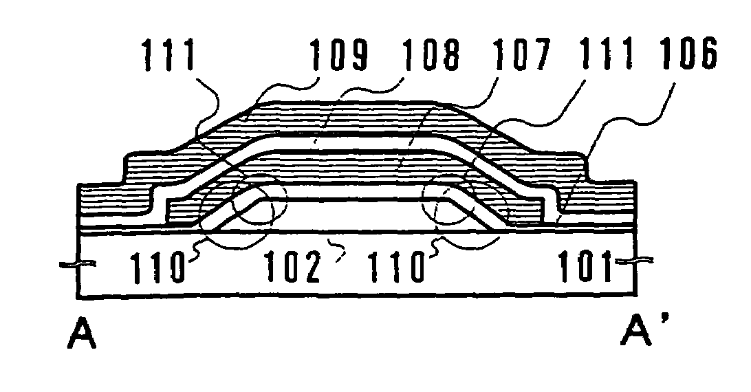
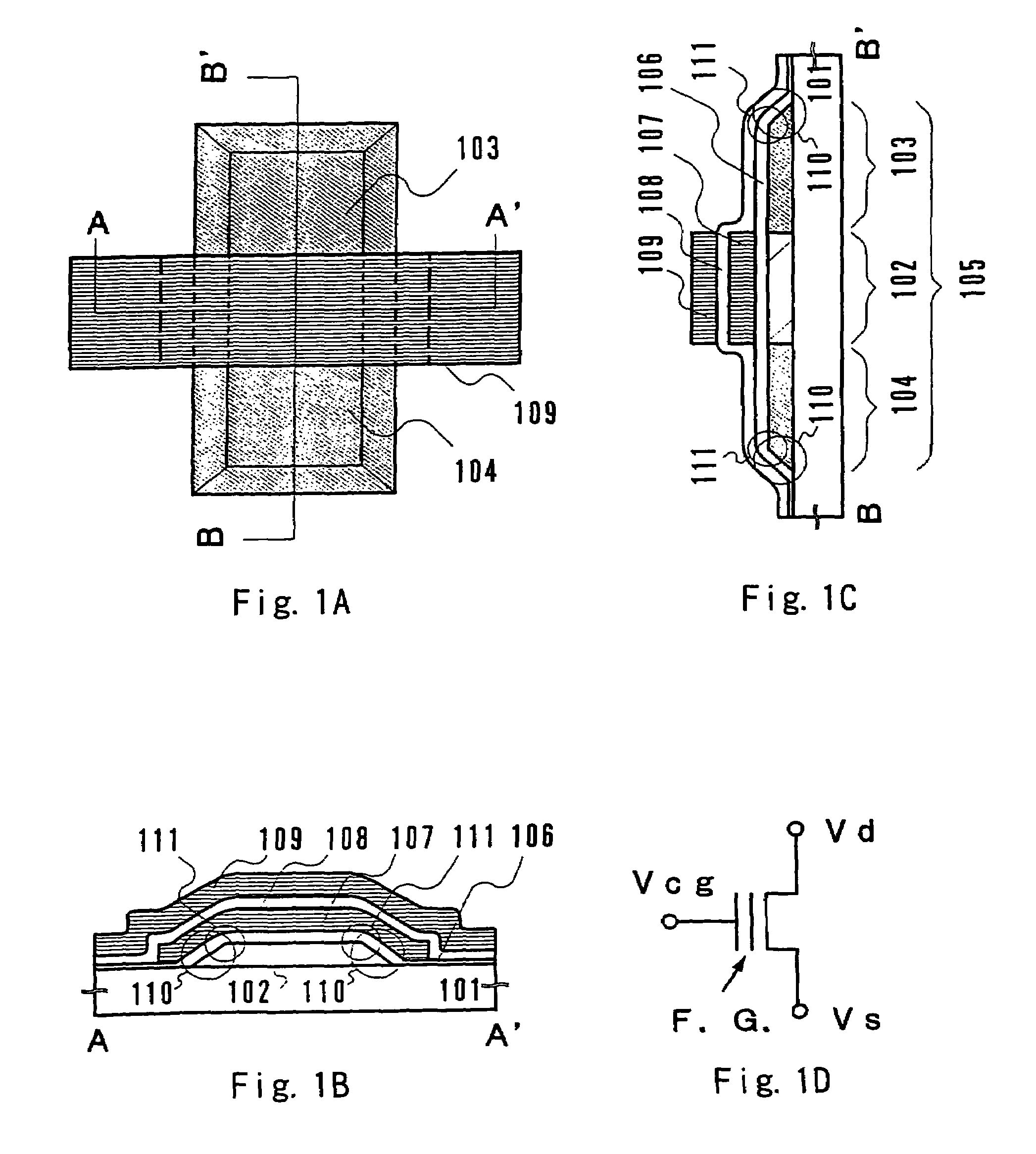
[0066]FIGS. 4A to 4E are sectional views each showing a major manufacturing step for manufacturing the n type memory TFT according to Embodiment Mode. These sectional views are taken along the line A-A′ in FIG. 1A.

[0067]First, a polycrystalline silicon thin film 402 with a thickness of 500 angstrom is formed on a substrate 401 having an insulating surface as shown in FIG. 4A. A quartz substrate, a silicon substrate with a thermal oxide film formed thereon, a ceramic substrate with a base film formed thereon, or the like can be used as the substrate 401 having an insulating surface. In this embodiment, a quartz substrate is employed.

[0068]The polycrystalline silicon thin film 402 may be formed directly by CVD apparatus or may be obtained by crystallizing an amorphous silicon thin film. When crystallizing amorphous silicon, any of furnace annealing, laser anne...

embodiment 2

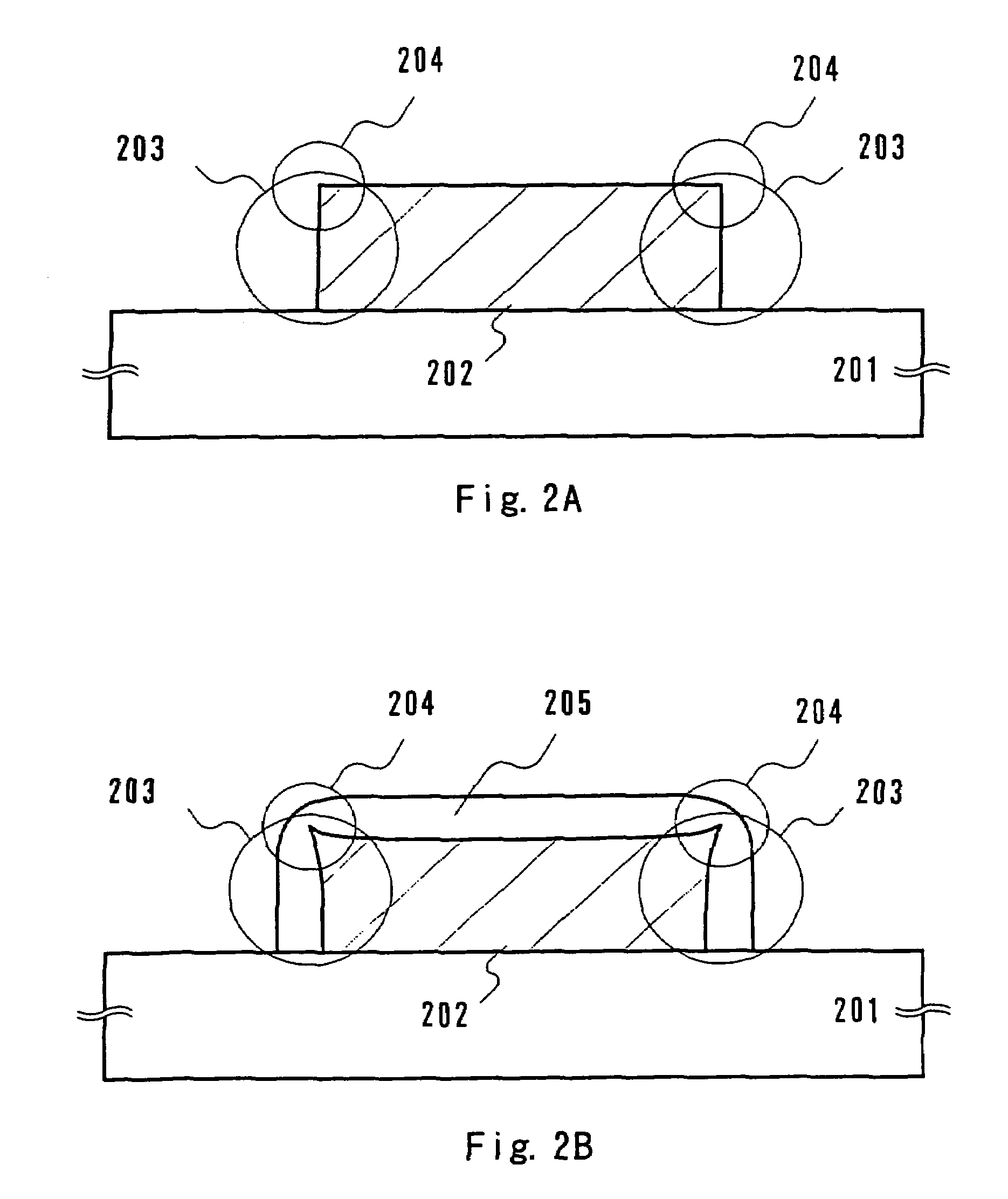
[0087]This embodiment describes a method of manufacturing a non-volatile memory in which active layer side ends are tapered and tiered to have two or more tiers.

[0088]The manufacturing steps of Embodiment 1 are employed here for steps from formation of a semiconductor thin film on a substrate having an insulating surface through formation of a photo resist having an active layer pattern. In the subsequent step of etching the semiconductor thin film, active layer side ends are tapered to have two tiers. The taper angle of the active layer side ends is set such that the upper tier has a smaller taper angle (preferably 20 to 50°) and the lower tier has a larger taper angle (preferably 40 to 70°). This prevents the active layer side ends from being pointed at the interface between the substrate having an insulating surface and the active layer.

[0089]The active layer side ends can be tapered to have two tiers by changing the selective ratio of the semiconductor thin film and photo resist...

embodiment 3

[0096]A memory TFT of the present invention can be applied to any known circuit structure that uses a non-volatile memory element. This embodiment describes a case of applying the present invention to a NOR flash memory.

[0097]FIG. 5A is a circuit diagram of a NOR flash memory circuit in which memory TFTs are arranged so as to form a matrix having m rows and n columns (m and n are integers each equal to or larger than 1). The conductivity type of the memory TFTs is either n type or p type.

[0098]In FIG. 5A, m memory TFTs 502 to 504 in the first column are connected to a bit line 501 indicated by B1. The m memory TFTs 502 to 504 respectively use as control gates m word lines 505 to 507 indicated by W1 to Wm. Similarly, m memory TFTs 509 to 511 in the n-th column are connected to a bit line 508 indicated by Bn. The m memory TFTs 509 to 511 respectively use as control gates the m word lines 506 to 507. In the memory TFTs 502 to 504 and 509 to 511, the terminals that are not connected to ...


PUM

PropertyMeasurementUnit
taper angleaaaaaaaaaa

Abstract

A non-volatile memory in which a leak current from an electric charge accumulating layer to an active layer is reduced and a method of manufacturing the non-volatile memory are provided. In a non-volatile memory made from a semiconductor thin film that is formed on a substrate (101) having an insulating surface, active layer side ends (110) are tapered. This makes the thickness of a first insulating film (106), which is formed by a thermal oxidization process, at the active layer side ends (110) the same as the thickness of the rest of the first insulating film. Therefore local thinning of the first insulating film does not take place. Moreover, the tapered active layer side ends hardly tolerate electric field concentration at active layer side end corners (111). Accordingly, a leak current from an electric charge accumulating layer (107) to the active layer (105) is reduced to improve the electric charge holding characteristic. As a result, the first insulating film can be further made thin to obtain a high performance non-volatile memory that operates at a low voltage and consumes less power.

Description

BACKGROUND OF THE INVENTION[0001]1. Field of the Invention[0002]The present invention relates to a non-volatile memory using a thin film transistor (TFT) and to a method of manufacturing the non-volatile memory.[0003]2. Description of Related Art[0004]The technique for forming a semiconductor thin film on an insulating substrate, especially the one for forming a silicon thin film on a glass substrate, is advancing at a remarkable pace in recent years. Conventionally, an insulated gate field effect transistor such as a MOS FET is formed on a single crystal semiconductor substrate. A TFT that has as its active layer a semiconductor thin film formed on an insulating substrate is expected to have low parasitic capacitance, high operation-speed, less power consumption, and a low manufacturing cost. Great hopes are laid on a system-on-glass in which those characteristics of TFT are utilized to integrate a system LSI on a glass substrate. To realize the system-on-glass, it is indispensable...

Claims


Application Information

Patent Timeline
Patent Type & Authority Patents(United States)
IPC IPC(8): H01L21/8247G02F1/1368H01L21/28H01L21/302H01L21/3065H01L21/314H01L21/336H01L27/10H01L27/115H01L29/423H01L29/786H01L29/788H01L29/792
CPCH01L21/28273H01L27/115H01L29/42324H01L29/7881H01L29/40114H10B69/00
Inventor KATO, KIYOSHIKUROKAWA, YOSHIYUKI
Owner SEMICON ENERGY LAB CO LTD
Why Eureka
Try Eureka