Method of manufacturing dielectric film of flash memory device

A technology for dielectric films and flash memory devices, which is applied in the field of manufacturing flash memory devices and can solve problems such as difficult formation of oxide films

Inactive Publication Date: 2006-12-27
SK HYNIX INC
View PDF0 Cites 0 Cited by
  • Summary
  • Abstract
  • Description
  • Claims
  • Application Information

AI Technical Summary

Problems solved by technology

It is therefore difficult to form an oxide film having goo...

Method used


Image

  • Method of manufacturing dielectric film of flash memory device
  • Method of manufacturing dielectric film of flash memory device
  • Method of manufacturing dielectric film of flash memory device

Examples


Embodiment Construction

[0028] Preferred embodiments according to the present invention will be described below with reference to the accompanying drawings. Since the preferred embodiments are provided to enable those skilled in the art to understand the present invention, they can be modified in various ways and the scope of the present invention is not limited to the preferred embodiments described below.

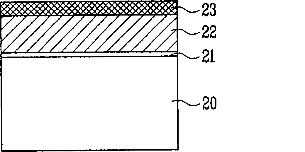
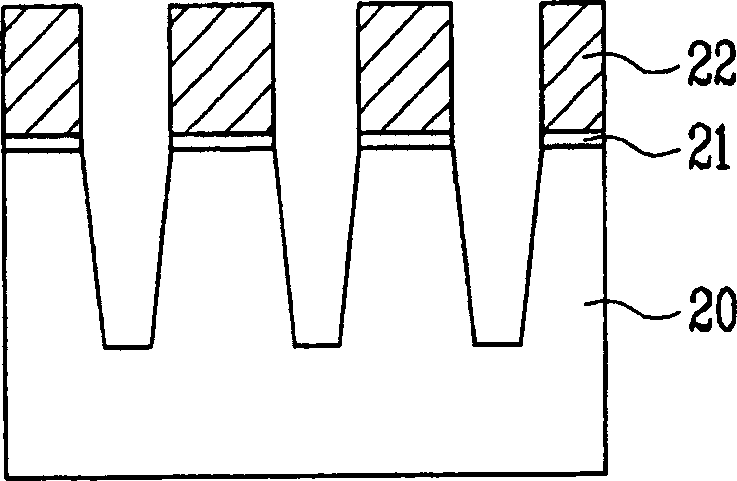
[0029] Figures 2A to 2I is a cross-sectional view for explaining a method of manufacturing a flash memory device according to an embodiment of the present invention.

[0030] Such as Figure 2A As shown, a screen oxide film 21 is formed on a semiconductor substrate 20 . An ion implantation process such as a well ion implantation process and a threshold voltage ion implantation process is then performed.

[0031] Before forming the barrier oxide film 21, SC-1 (NH 4 OH / H 2 o 2 / H 2 A mixture of O) and HF or a mixture of SC-1 and BOE diluted with distilled water in a ratio of 100:1 or 300:1...


PUM


Abstract

A method of manufacturing a dielectric film of a flash memory device, including the steps of providing a semiconductor substrate having floating gates formed therein, performing an oxidization process in a decompression state to form a first oxide film of a thin film on the semiconductor substrate including the floating gates, and sequentially forming a nitride film and a second oxide film on the first oxide film to form a dielectric film having the first oxide film, the nitride film and the second oxide film.

Description

technical field [0001] The present invention relates to a method of manufacturing a flash memory device, and more particularly, to a method of forming a dielectric film formed between a floating gate and a control gate of the flash memory device. Background technique [0002] Generally, the gate of a flash memory device has a structure including a tunnel oxide film 11, a floating gate 12, a dielectric film 13, and a control gate 14, all of which are formed on a silicon substrate 10, such as figure 1 shown. Reference numeral 15 denotes an isolation film. [0003] The programming, erasing and reading operations of the flash memory device constructed as above are performed in such a manner that by applying an appropriate bias voltage to the control gate 14 and the silicon substrate 10, electrons are injected into or taken out from the floating gate 12 . [0004] Dielectric film 13 has an oxide-nitride-oxide (ONO) structure in which a first oxide film 13a, a nitride film 13b,...

Claims


Application Information

Patent Timeline
IPC IPC(8): H01L21/336H01L21/283H01L21/314
CPCH01L29/66825H01L21/02255H01L21/02211H01L27/11521H01L21/02337H01L21/02271H01L21/02233H01L21/31662H01L21/02126H01L27/115H01L21/3144H10B69/00H10B41/30H01L27/105H10B99/00
Inventor 朱光喆
Owner SK HYNIX INC
Why Eureka
Try Eureka