Composite hard mask with upper sacrificial dielectric layer for the patterning and etching of nanometer size MRAM devices

a technology of sacrificial dielectric layer and nanometer-size mram, which is applied in the direction of thin material processing, semiconductor devices, electrical apparatus, etc., can solve the problems of limiting the critical dimension (cd) of mram devices, affecting the production efficiency of ic devices such as spin torque mram, and affecting the quality of ic devices. , to achieve the effect of preventing metal etch residue formation

Active Publication Date: 2014-05-13
TAIWAN SEMICON MFG CO LTD
View PDF10 Cites 77 Cited by
  • Summary
  • Abstract
  • Description
  • Claims
  • Application Information

AI Technical Summary

Benefits of technology

[0013]One objective of the present invention is to provide a MTJ hard mask design that prevents metal etch residue formation and build up on sidewalls of a MTJ during fabrication of a MRAM device.
[0014]A second objective of the present invention is to provide a MTJ hard mask configuration according to the first objective that is thin enough to enable a thin overlying photoresist layer to be patterned with an acceptable process latitude but is also thick enough to prevent electric shorting between an overlying bit line and the MTJ.
[0016]According to a first embodiment, these objectives are achieved by providing a substrate comprised of a bottom electrode layer on which a MRAM or STT-MRAM structure is to be fabricated. A MTJ is formed by first depositing a stack of layers on the bottom electrode layer. In one aspect, the MTJ stack has a bottom spin valve configuration in which a seed layer, AFM layer, synthetic anti-ferromagnetic (SyAF) pinned layer, tunnel barrier layer, and a free layer are sequentially formed. A key feature is the formation of a composite hard mask comprised of a thin non-magnetic metal spacer on the free layer, a middle conductive layer that has high etch selectivity with respect to underlying MTJ layers, and an upper sacrificial dielectric layer. The non-magnetic metal spacer serves as an etch stop for the etch transfer process through the middle conductive layer and also prevents a metal such as Ta in the conductive layer from migrating into the free layer and causing a lower magnetoresistive (MR) ratio. The middle conductive layer becomes the top layer in the hard mask after the MTJ stack of layers is etched. In a second embodiment, the non-magnetic metal spacer may be omitted such that the conductive layer contacts the free layer in the MTJ.

Problems solved by technology

A tapered profile can not only lead to electrical shorting issues but also limits further reduction of critical dimension (CD) of MRAM devices and makes it nearly impossible to manufacture very high density IC devices such as spin torque MRAM.
On the other hand, the heavy metal layer should not be too thick since a thicker photoresist mask will be required for pattern transfer and as the photoresist thickness increases there is a greater tendency for the photoresist pattern to collapse which drives more rework and higher cost.
Formation and buildup of metal etch residue significantly affects the shape integrity of MTJ structures which in turn affects MRAM device performance.
Consequently, MTJ shape integrity is lost and MRAM device performance suffers.
In a manufacturing environment, the MTJ shapes and defects shown in FIG. 1 would be unacceptable and substrate 8 would require rework.
Unfortunately, a thin Ta hard mask leads to potential issues of electrical shorting as mentioned previously and limits the amount of etch time available to transfer the hard mask pattern through the MTJ stack of layers because the hard mask erodes during the pattern transfer process.
Overall, the entire patterning sequence involves several additional steps than in a single composite hard mask scheme and there is no protection of the Ta hard mask during etching of MTJ layers.

Method used


Image

  • Composite hard mask with upper sacrificial dielectric layer for the patterning and etching of nanometer size MRAM devices
  • Composite hard mask with upper sacrificial dielectric layer for the patterning and etching of nanometer size MRAM devices
  • Composite hard mask with upper sacrificial dielectric layer for the patterning and etching of nanometer size MRAM devices

Examples


Embodiment Construction

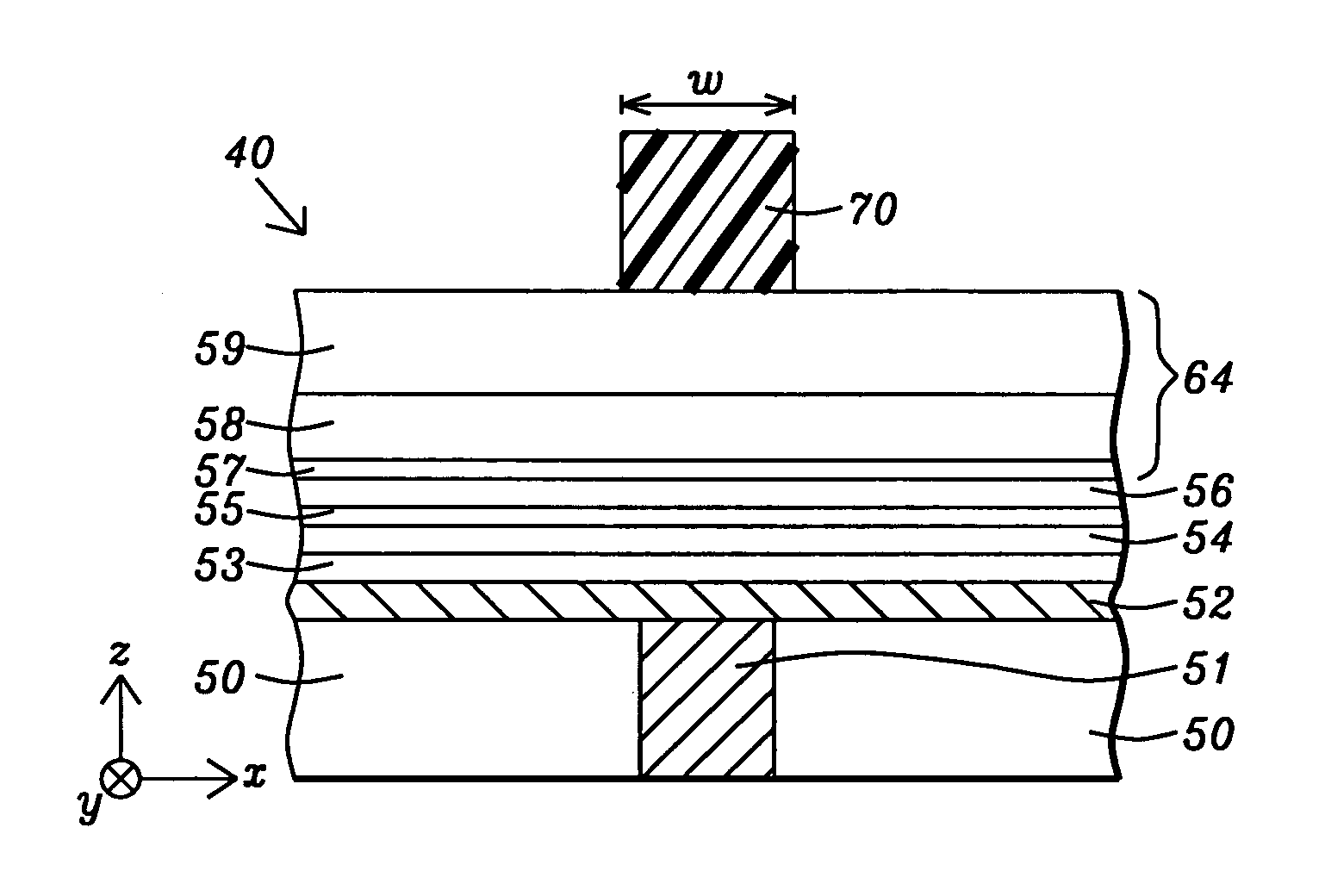
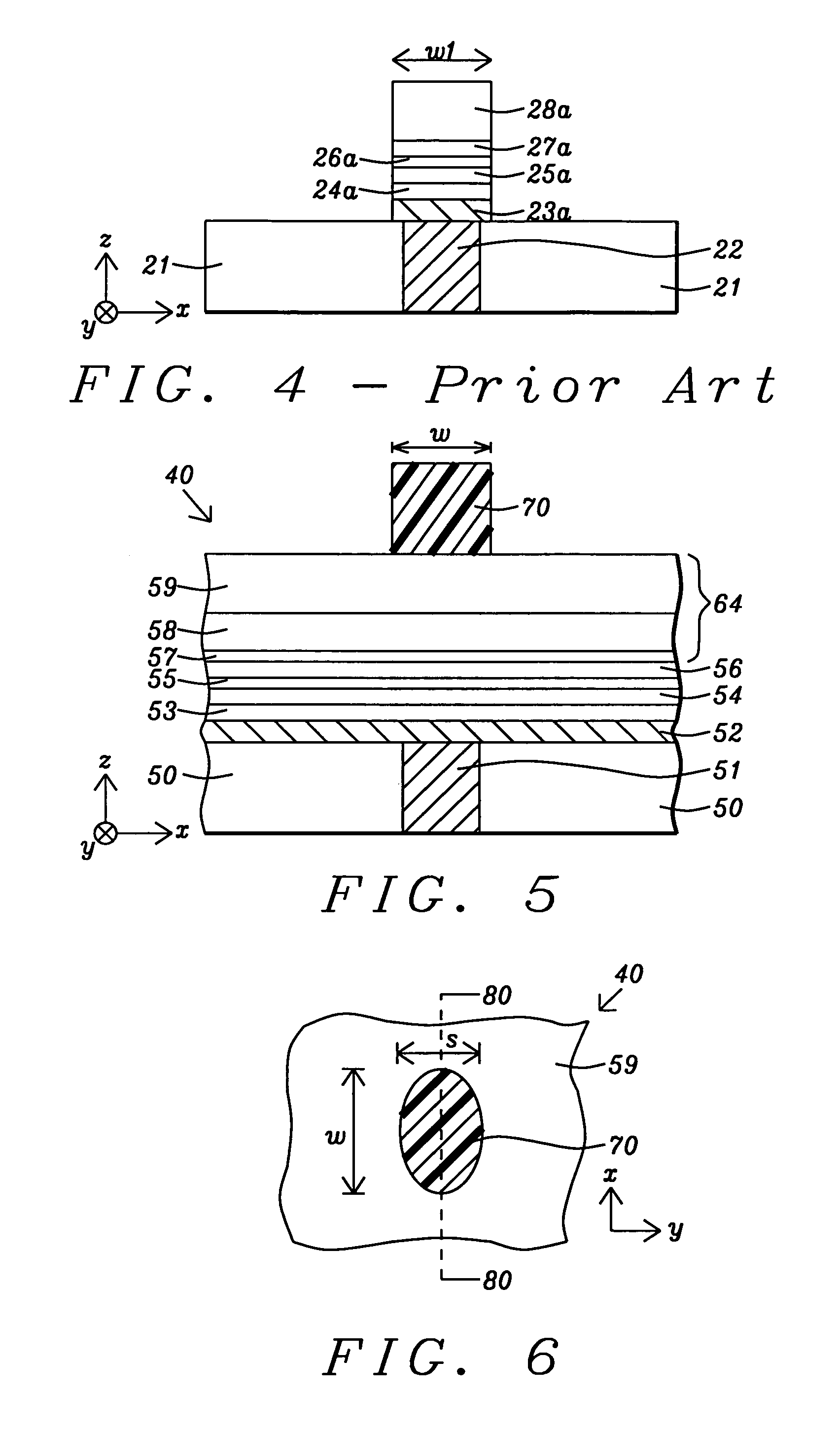
[0028]The present invention is a hard mask design and a method of using the hard mask to form MTJ elements in advanced memory devices including MRAM and STT-MRAM. The drawings are provided by way of example and are not intended to limit the scope of the invention. Although a bottom spin valve MTJ structure is described in the exemplary embodiment, the present invention also encompasses other MTJ configurations such as top spin valve and multi-layer spin valve structures. The present invention also anticipates that the hard axis and easy axis dimensions of a MTJ element may be formed in separate steps. In this case, the sequence of photoresist patterning and subsequent etch steps outlined in the exemplary embodiment may be used to define a first CD that is an x-axis dimension of a MTJ, for example. Then the sequence of photoresist patterning and etch steps may be repeated to define a second CD that is a y-axis dimension of the MTJ. Only one MTJ is shown in the exemplary embodiment in...


PUM

PropertyMeasurementUnit
thicknessaaaaaaaaaa
thicknessaaaaaaaaaa
thicknessaaaaaaaaaa

Abstract

A composite hard mask is disclosed that prevents build up of metal etch residue in a MRAM device during etch processes that define an MTJ shape. As a result, MTJ shape integrity is substantially improved. The hard mask has a lower non-magnetic spacer, a middle conductive layer, and an upper sacrificial dielectric layer. The non-magnetic spacer serves as an etch stop during a pattern transfer with fluorocarbon plasma through the conductive layer. A photoresist pattern is transferred through the dielectric layer with a first fluorocarbon etch. Then the photoresist is removed and a second fluorocarbon etch transfers the pattern through the conductive layer. The dielectric layer protects the top surface of the conductive layer during the second fluorocarbon etch and during a substantial portion of a third RIE step with a gas comprised of C, H, and O that transfers the pattern through the underlying MTJ layers.

Description

RELATED PATENT APPLICATION[0001]This application is related to the following: Ser. No. 11 / 901,999, filing date Sep. 20, 2007; assigned to a common assignee and herein incorporated by reference in its entirety.FIELD OF THE INVENTION[0002]The invention relates to a composite hard mask used in the fabrication of a magnetic tunnel junction (MTJ) element and includes an upper sacrificial dielectric layer to prevent a lower metal layer from forming metal residues during an etch transfer step thereby resulting in more uniform MTJ shapes which improves device performance.BACKGROUND OF THE INVENTION[0003]Magnetoresistive Random Access Memory (MRAM), based on the integration of silicon CMOS with MTJ technology, is a major emerging technology that is highly competitive with existing semiconductor memories such as SRAM, DRAM, Flash, etc. A MRAM device is generally comprised of an array of parallel first conductive lines on a horizontal plane, an array of parallel second conductive lines on a se...

Claims


Application Information

Patent Timeline
Patent Type & Authority Patents(United States)
IPC IPC(8): H01L21/302H01L21/00
CPCH01L43/12Y10T428/31678Y10T428/12535Y10T428/31504Y10T428/266Y10T428/24975H10N50/01
Inventor BELEN, RODOLFOXIAO, RONGFUZHONG, TOMKULA, WITOLDTORNG, CHYU-JIUH
Owner TAIWAN SEMICON MFG CO LTD
Why Eureka
Try Eureka