Chamber configuration for confining a plasma

a chamber configuration and plasma technology, applied in plasma techniques, energy-based chemical/physical/physico-chemical processes, coatings, etc., can solve problems such as process performance variations, chamber or chamber parts life reduction, etc., and achieve the effect of reducing the effect of plasma forming components

Inactive Publication Date: 2005-03-29
LAM RES CORP
View PDF20 Cites 74 Cited by
  • Summary
  • Abstract
  • Description
  • Claims
  • Application Information

AI Technical Summary

Benefits of technology

The invention relates, in one embodiment, to a plasma confining assembly for minimizing unwanted plasma formations in regions outside of a process region in a process chamber. The assembly includes a first confining element positioned proximate the periphery of the process region. The first confining element includes an exposed conductive surface that is electrically grounded. The assembly further includes a second confining element positioned proximate the periphery of the process region and spaced apart from the first confining element. The second confining element includes an exposed insulating surface, which is configured for covering a conductive portion that is electrically grounded. The first confining element and the second confining element are arranged to substantially reduce the effects of plasma forming components (e.g., charged particles and / or electric fields) that pass therebetween.
In other embodiments, the plasma confining assembly additionally includes a third confining element formed from an insulating material. The third confining element is disposed between the first confining element and the second confining element and proximate the periphery of the process region. The third confinement element is arranged to physically contain a plasma inside the process region and to substantially reduce the effects of plasma forming components that pass between the first confining element and the second confining element.
The invention relates, in another embodiment, to a plasma reactor for processing a substrate. The plasma reactor includes a chamber having chamber walls. The plasma reactor further includes an electrode arrangement configured for generating an electric field, which is sufficiently strong to both ignite and sustain a plasma for the processing within the chamber. The electrode arrangement includes a first electrode and a second electrode, which are spaced apart thereby defining a process region therebetween. The plasma reactor additionally includes a plasma confinement assembly for preventing the plasma from forming outside of the process region. The plasma confinement assembly includes a first ring, which is configured to surround the first electrode, and a second ring, which is configured to surround the second electrode. The first ring includes an exposed conductive surface that is electrically grounded, and the second ring includes an exposed insulating surface covering a non exposed conductive element that is grounded. The plasma confinement assembly is arranged to substantially reduce the effects of plasma forming components that pass between the first confinement ring and the second confinement ring.

Problems solved by technology

If the plasma reaches these areas, etch, deposition and / or corrosion of the areas may ensue, which may lead to particle contamination inside the process chamber, and / or which may reduce the lifetime of the chamber or chamber parts.
Furthermore, a non-confined plasma may form a non uniform plasma, which may lead to variations in process performance.

Method used


Image

  • Chamber configuration for confining a plasma
  • Chamber configuration for confining a plasma
  • Chamber configuration for confining a plasma

Examples


Embodiment Construction

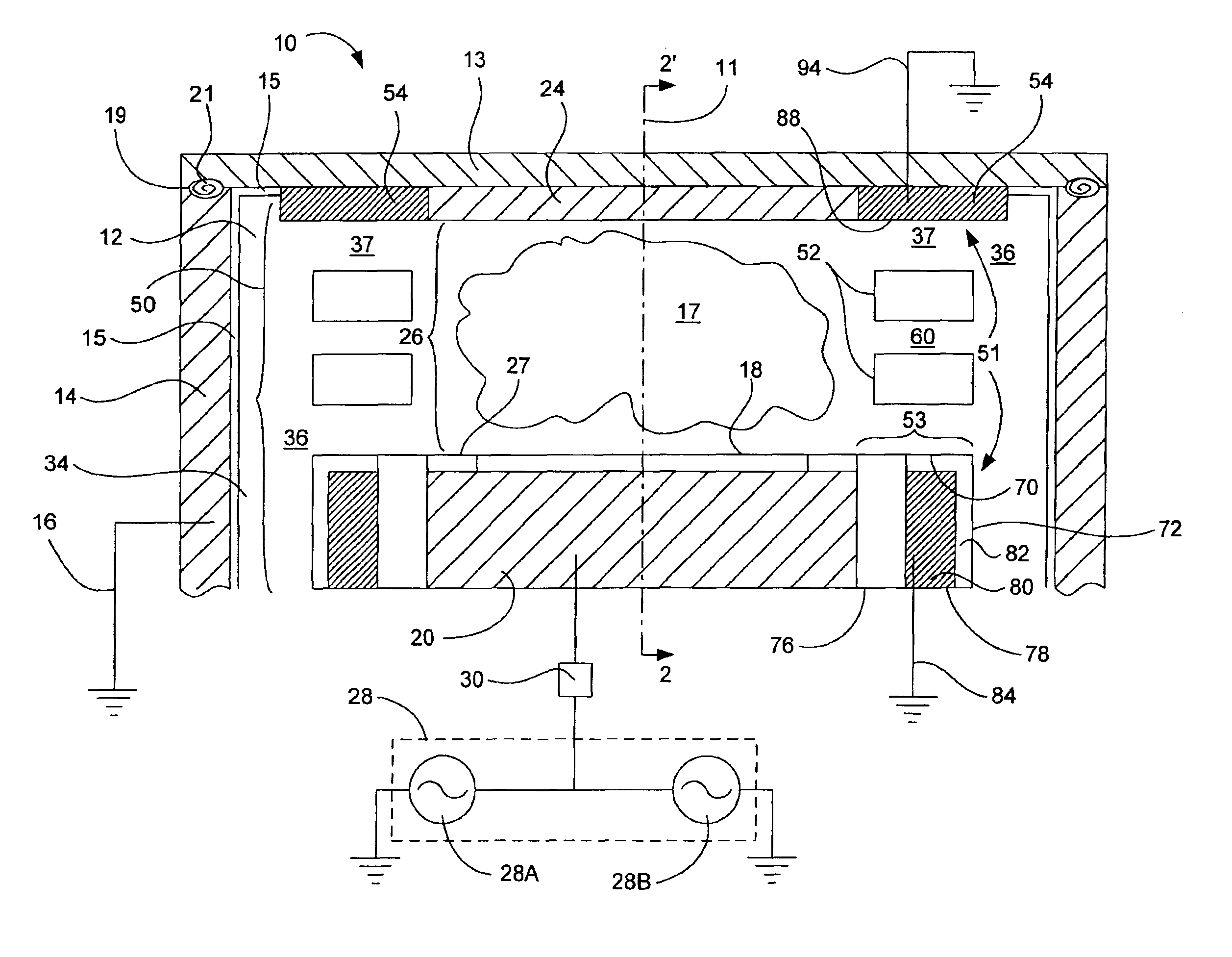
The present invention will now be described in detail with reference to a few preferred embodiments thereof as illustrated in the accompanying drawings. In the following description, numerous specific details are set forth in order to provide a thorough understanding of the present invention. It will be apparent, however, to one skilled in the art, that the present invention may be practiced without some or all of these specific details. In other instances, well known process steps have not been described in detail in order not to unnecessarily obscure the present invention.

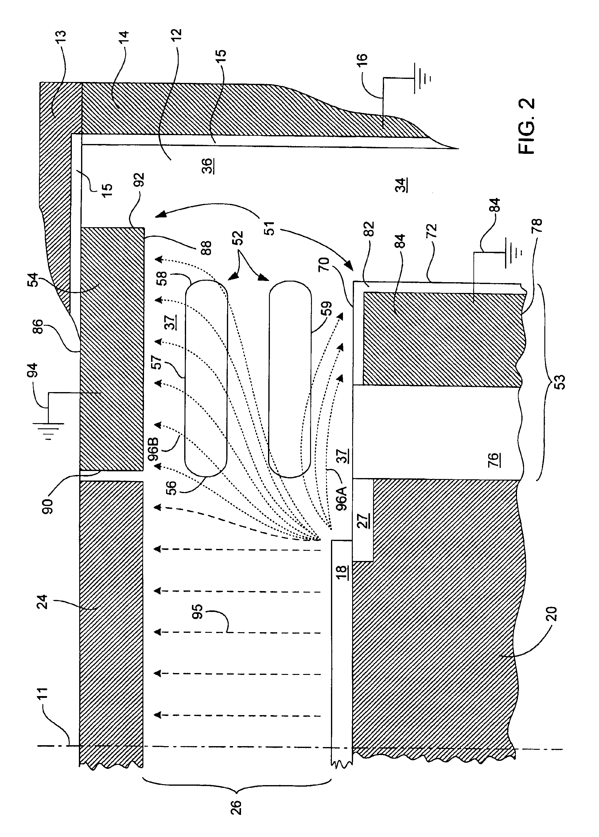
It has been discovered that unwanted discharges or plasmas may be encountered when large charged particle fluxes and / or large electric fields are present in regions outside of the process region of the process chamber. As the term is employed herein, the process region refers to the region of the process chamber used for processing a substrate, for example, the area directly above the substrate. With regards to c...


PUM

PropertyMeasurementUnit
frequencyaaaaaaaaaa
frequencyaaaaaaaaaa
conductiveaaaaaaaaaa

Abstract

A plasma confining assembly for minimizing unwanted plasma formations in regions outside of a process region in a process chamber is disclosed. The plasma confining assembly includes a first confining element and second confining element positioned proximate the periphery of the process region. The second confining element is spaced apart from the first confining element. The first confining element includes an exposed conductive surface that is electrically grounded and the second confining element includes an exposed insulating surface, which is configured for covering a conductive portion that is electrically grounded. The first confining element and the second confining element substantially reduce the effects of plasma forming components that pass therebetween. Additionally, the plasma confining assembly may include a third confining element, which is formed from an insulating material and disposed between the first confining element and the second confining element, and proximate the periphery of the process region. The third confining element further reduces the effects of plasma forming components that pass between the first confining element and the second confining element.

Description

BACKGROUND OF THE INVENTIONThe present invention relates to apparatus and methods for processing substrates such as semiconductor substrates for use in IC fabrication or glass panels for use in flat panel display applications. More particularly, the present invention relates to improved techniques for controlling plasma formation in a process chamber of a plasma reactor.The use of plasma-enhanced processes in the manufacture of semiconductor-based products (such as integrated circuits or flat panel displays) is well known. In general, plasma-enhanced processes involve processing a substrate in a process chamber of a plasma reactor. In most plasma reactors, a plasma may be ignited and sustained by supplying a gas containing appropriate etchant or deposition source gases into the process chamber and applying energy to those source gases to respectively etch or deposit a layer of material on the surface of the substrate. By way of example, capacitive plasma reactors have been widely us...

Claims


Application Information

Patent Timeline
Patent Type & Authority Patents(United States)
IPC IPC(8): H01J37/32B01J19/08C23F4/00H05H1/46H01L21/205H01L21/3065
CPCH01J37/32082H01J37/32871H01J37/32623H01L21/3065
Inventor CHEN, JIAN J.SRINIVASAN, MUKUNDLENZ, ERIC H.
Owner LAM RES CORP
Why Eureka
Try Eureka