SOI semiconductor integrated circuit for eliminating floating body effects in SOI MOSFETs and method of fabricating the same

Inactive Publication Date: 2002-12-24
SAMSUNG ELECTRONICS CO LTD
View PDF8 Cites 81 Cited by
  • Summary
  • Abstract
  • Description
  • Claims
  • Application Information

AI Technical Summary

Benefits of technology

FIG. 2B is a plot illustrating the dynamic leakage current occurring

Problems solved by technology

Despite the above outstanding features of SOI devices, SOI integrated circuits have suffered some lack of commercial success due to technical problems in material processing and device design.
However, since the dynamic leakage current cannot be avoided between source and drain when the gate voltage is high while keeping source and drain low, they pointed out that their approach is only applicable to the low voltage operation.
However, it should b

Method used


Image

  • SOI semiconductor integrated circuit for eliminating floating body effects in SOI MOSFETs and method of fabricating the same
  • SOI semiconductor integrated circuit for eliminating floating body effects in SOI MOSFETs and method of fabricating the same
  • SOI semiconductor integrated circuit for eliminating floating body effects in SOI MOSFETs and method of fabricating the same

Examples


Example

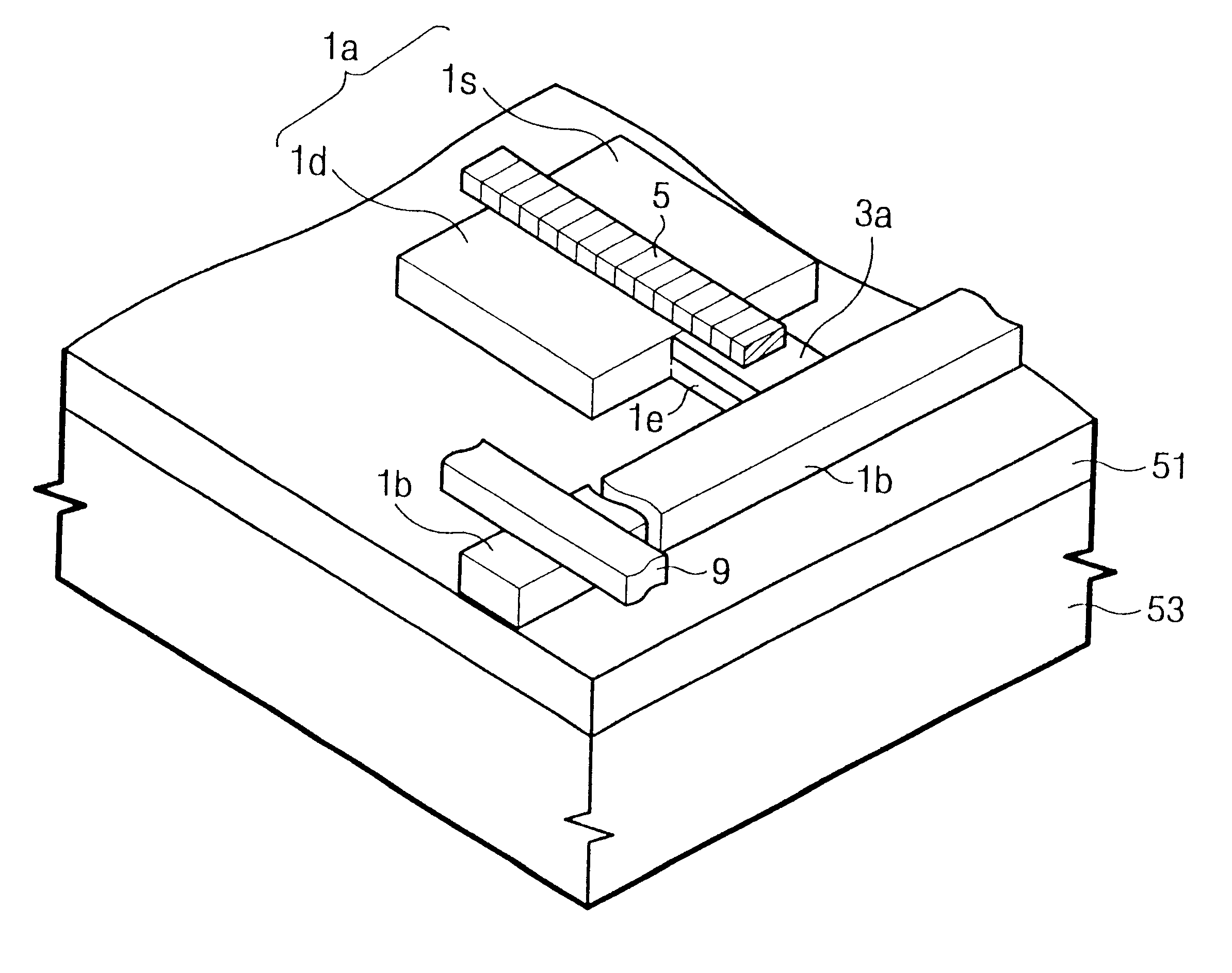
The present invention will be explained in detail with reference to the accompanying drawings. FIGS. 4A and 5 are a top view and a perspective view, respectively, showing a portion of an SOI integrated circuit according to an embodiment of the present invention. An SOI integrated circuit in accordance with the invention including N-MOSFETs will be described with reference to FIGS. 4A and 5. However, the present invention is applicable to SOI integrated circuits including P-MOSFETs. Also, the SOI integrated circuit of the present invention could be implemented using N-MOSFETs and P-MOSFETs.

Referring to FIGS. 4A and 5, at least one isolated transistor active region 1a is located at a predetermined region of an SOI substrate. A body line 1b is disposed at one side of the transistor active region Ia. In detail, the transistor active region 1a may be disposed at one side of the body line 1b. The body line 1b is electrically connected to a body extension 1e which is extended from a sidewa...


PUM


Abstract

A silicon-on-insulator (SOD integrated circuit and a method of fabricating the SOI integrated circuit are provided. At least one isolated transistor active region and a body line are formed on an SOI substrate. The transistor active region and the body line are surrounded by an isolation layer which is in contact with a buried insulating layer of the SOI substrate. A portion of the sidewall of the transistor active region is extended to the body line. Thus, the transistor active region is electrically connected to the body line through a body extension. The body extension is covered with a body insulating layer. An insulated gate pattern is formed over the transistor active region, and one end of the gate pattern is overlapped with the body insulating layer.

Description

The present invention generally relates to silicon-on-insulator (SOI) technology, and more particularly to an SOI semiconductor integrated circuit for eliminating floating body effects in SOI MOSFETs and a method of fabricating the same.DESCRIPTION OF THE RELATED ARTIn the semiconductor manufacturing industry, there has been a great deal of attention paid to reducing parasitic capacitance and resistance to increase the operating speed of semiconductor integrated circuits. SOI MOSFETs have been demonstrated to be superior to bulk silicon MOSFETs in terms of low power, high speed very large scale integration (VLSI) applications because of their inherent merits such as less junction capacitance and better device isolation. In addition, there are many advantages in SOI devices such as better immunity to soft errors, reduction in dynamic power, improvement in latch-up resistance even with increased packing density. Despite the above outstanding features of SOI devices, SOI integrated cir...

Claims


Application Information

Patent Timeline
IPC IPC(8): H01L29/66H01L29/786H01L29/78
CPCH01L29/78615H01L29/78
Inventor KIM, YOUNG-WUGKIM, BYUNG-SUNKANG, HEE-SUNGKO, YOUNG-GUNPARK, SUNG-BAE
Owner SAMSUNG ELECTRONICS CO LTD
Why Eureka
Try Eureka