Semiconductor device and method for fabricating the same

a technology of semiconductor devices and semiconductors, applied in semiconductor devices, electrical equipment, transistors, etc., can solve problems such as defective contacts to the source/drain region of memory cell transistors, and achieve the effect of suppressing defective contacts

Inactive Publication Date: 2005-09-01
FUJITSU SEMICON LTD
View PDF3 Cites 74 Cited by
  • Summary
  • Abstract
  • Description
  • Claims
  • Application Information

AI Technical Summary

Benefits of technology

[0012] According to the present invention, in a non-volatile semiconductor memory having the double sidewall spacer structure including the first sidewall spacer and the second sidewall spacer sequentially laid the latter on the former, the film thickness of the silicon oxide film between the second sidewall spacer and the semiconductor substrate is smaller than the film thickness of the silicon oxide film between the first sidewall spacer and the semiconductor substrate, whereby the silicon oxide film on the source / drain regions of the non-volatile semiconductor memory can be completely removed by the usual step of fabricating a peripheral transistor and the pre-treatment of the salicide steps. Accordingly, the failure to form the silicide film on the source / drain regions of the non-volatile semiconductor memory can be prevented, and the defective contact can be suppressed.

Problems solved by technology

However, the inventors of the present application have made earnest studies of such double sidewall spacer structure and found that defective contacts to the source / drain regions of the memory cell transistors take place.

Method used


Image

  • Semiconductor device and method for fabricating the same
  • Semiconductor device and method for fabricating the same
  • Semiconductor device and method for fabricating the same

Examples


embodiment

[0041] The semiconductor device and the method for fabricating the same according to one embodiment of the present invention will be explained with reference to FIGS. 1 to 22C.

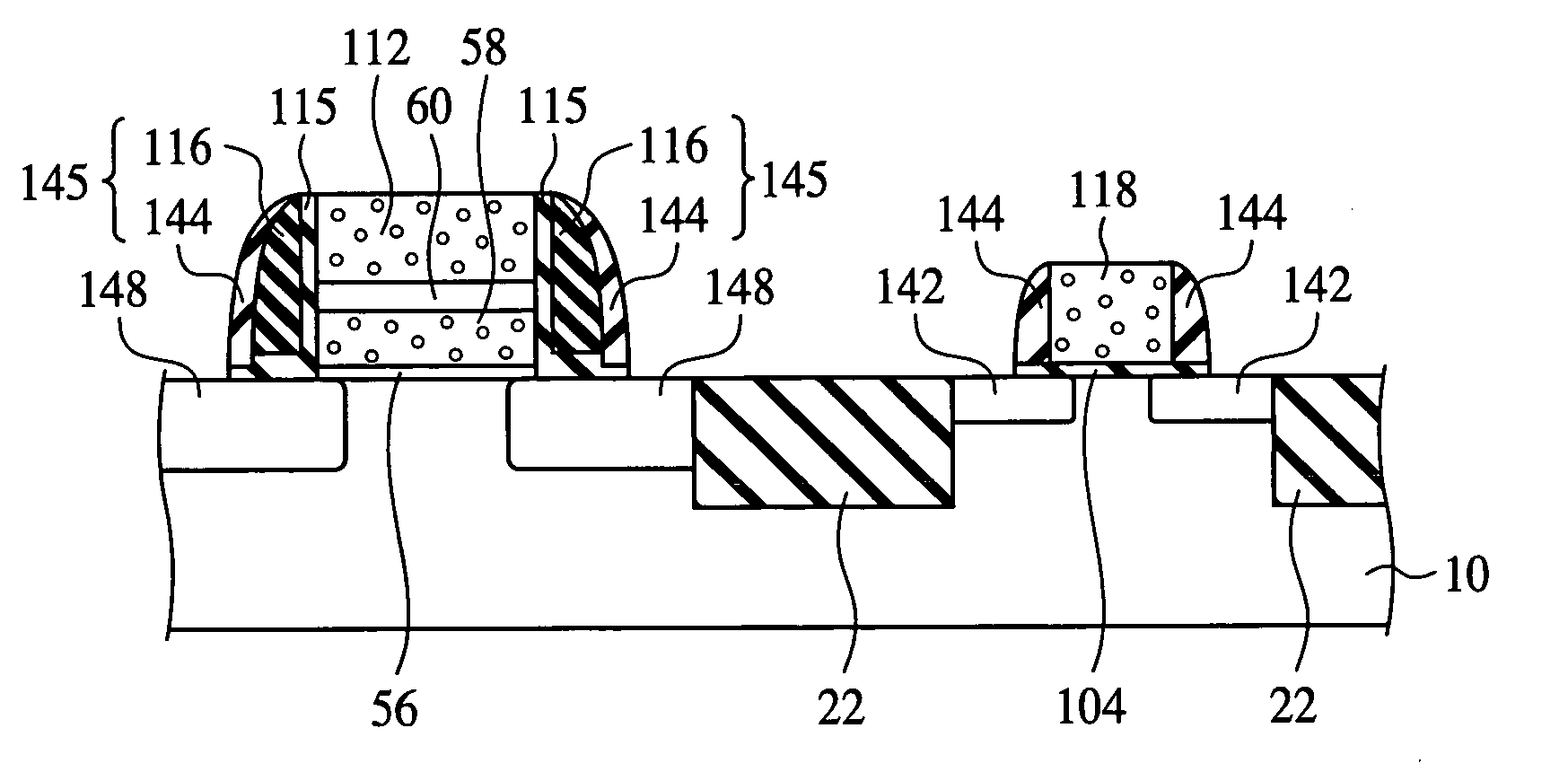
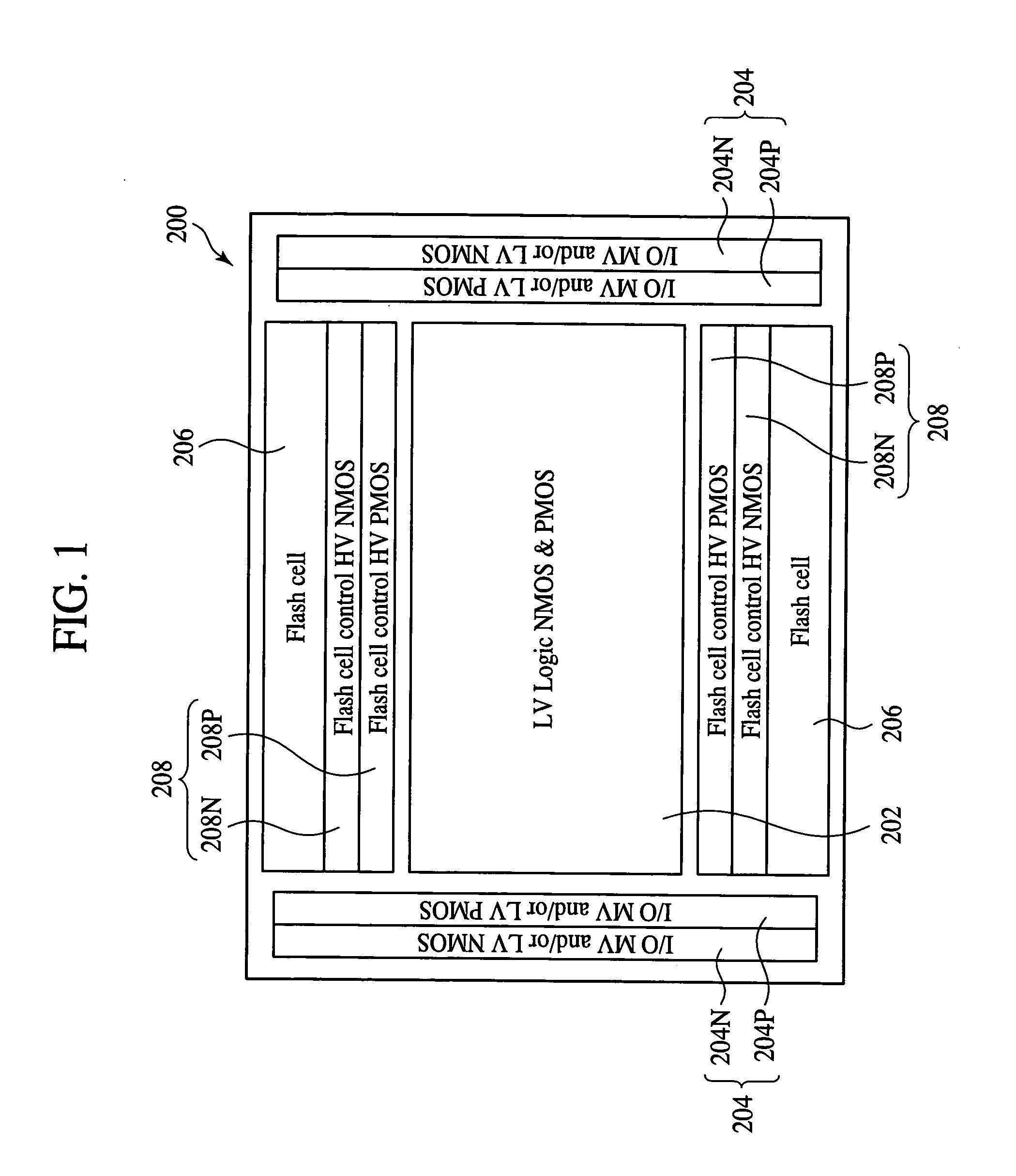
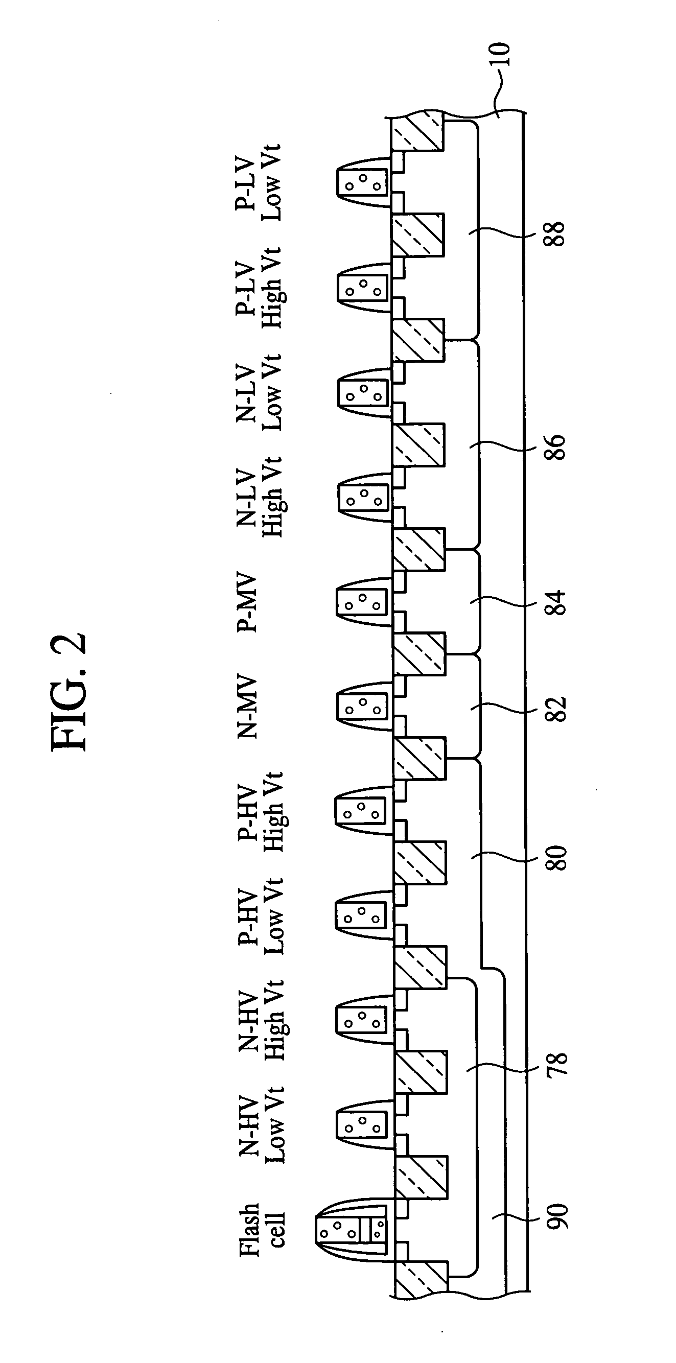
[0042]FIG. 1 is a chip conceptual view of the semiconductor device according to the present embodiment, which shows the structure thereof. FIG. 2 is a conceptual sectional view of 11 kinds of transistors used in the semiconductor device according to the present embodiment. FIG. 3 is a diagrammatic sectional view of the semiconductor device according to the present embodiment, which shows the structure thereof. FIGS. 4A to 22C are sectional views of the semiconductor device according to the present embodiment in the steps of the method for fabricating the semiconductor device, which show the method.

[0043] As shown in FIG. 1, the semiconductor device according to the present embodiment is a logic semiconductor device combined with a flash memory and comprises a main logic circuit unit 202, an input / output circ...


PUM


Abstract

The semiconductor device comprises a gate electrode 112 formed over a semiconductor substrate 10, a sidewall spacer 116 formed on the sidewall of the gate electrode 112, a sidewall spacer 144 formed on the side wall of the gate electrode 112 with the sidewall spacer 116 formed on, and an oxide film 115 formed between the sidewall spacer 116 and the sidewall spacer 144, and the semiconductor substrate 10. The film thickness of the oxide film 115 between the sidewall spacer 144 and the semiconductor substrate 10 is thinner than the film thickness of the oxide film 115 between the sidewall spacer 116 and the semiconductor substrate 10.

Description

CROSS-REFERENCE TO RELATED APPLICATIONS [0001] This application is based upon and claims the benefit of priority from the prior Japanese Patent Application No. 2004-54618, filed on Feb. 27, 2004, the entire contents of which are incorporated herein by reference. BACKGROUND OF THE INVENTION [0002] The present invention relates to a semiconductor device and a method for fabricating the semiconductor device, more specifically, a logic semiconductor device combined with a non-volatile memory and a method for fabricating the same. [0003] Logic semiconductor devices combined with non-volatile memory devices form product fields, as of CPLD (Complex Programmable Logic Device) and FPGA (Field Programmable Gate Array), and because of their characteristic of programmability, so far have formed large markets because of their characteristic, programmability. [0004] The logic semiconductor device combined with a non-volatile memory has, in addition to flash memory cells, high-voltage transistors ...

Claims


Application Information

Patent Timeline
Patent Type & Authority Applications(United States)
IPC IPC(8): H01L27/10H01L21/336H01L21/8242H01L21/8247H01L27/115H01L29/00H01L29/788H01L29/792
CPCH01L27/115H01L27/11526H01L29/6659H01L29/6656H01L27/11546H10B41/40H10B41/49H10B69/00
Inventor NAKAGAWA, SHINICHI
Owner FUJITSU SEMICON LTD
Why Eureka
Try Eureka