Field-effect transistor, display element, image display device, and system

a field-effect transistor and display element technology, applied in semiconductor devices, instruments, electrical devices, etc., can solve the problems of limiting the mobility of a-igzo, tfts with tfts having a-igzo as the active layer having low stability, so as to achieve more stable resultant properties and higher valen

Active Publication Date: 2020-09-24
RICOH KK
View PDF0 Cites 0 Cited by
  • Summary
  • Abstract
  • Description
  • Claims
  • Application Information

AI Technical Summary

Benefits of technology

[0034]A field-effect transistor of the present disclosure includes a semiconductor layer formed of an n-type metal oxide semiconductor and if necessary further includes a gate electrode, a source electrode, a drain electrode, a gate insulating film, and other components.
[0035]The semiconductor layer (active layer) is, for example, a layer provided to be adjacent to the source electrode and the drain electrode.
[0036]In the field-effect transistor of the present disclosure, the n-type metal oxide semiconductor forming the semiconductor layer contains indium oxide, and the indium oxide is n-type doped through introduction of one or more kinds of cations as dopants. This n-type metal oxide semiconductor has a peak detected at an angle corresponding to a (222) plane of indium oxide having a bixbite structure in an X-ray diffraction method using a two-dimensional detector.
[0037]In this substitution-doped n-type metal oxide semiconductor, some of the indium sites of the indium oxide that is the mother phase are replaced with ions of dopants having a higher valence. Excessive electrons released due to the difference in valances serve as carriers of n-type conduction. When the carrier electrons generated by such substitutional doping are responsible for semiconductor properties, the resultant properties become more stable. This is because the number of carrier electrons derived from oxygen vacancy easily changes by influences of, for example, oxidation / reduction reactions and oxygen adsorption onto the film surface due to the exchange of oxygen between the semiconductor and the outside (the atmosphere and adjacent layers) whereas the number of carrier electrons derived from substitutional doping is relatively unaffected by such state changes.
[0038]Regarding substitutional doping, it is known that even if substitutional doping is performed when the amorphous nature of an oxide semiconductor serving as the mother phase is high, the resultant structure changes to be in a locally stable state, so that no carrier is generated. The present inventors performed X-ray diffraction measurement on the n-type metal oxide semiconductor, but did not obtain any information on its crystallinity or amorphous nature. This is because a suitable film thickness of the n-type metal oxide semiconductor as the active layer of TFT is small; i.e., 30 nm or less in many cases, so that no peak can be observed in X-ray diffraction even in the crystalline state. As a result of the studies by the present inventors, it has been found that crystallinity can be assessed by an X-ray diffraction method using a two-dimensional detector, and when a peak is detected at an angle corresponding to a (222) plane of indium oxide having a bixbite structure, a preferable state is achieved where carriers are generated by substitutional doping effectively working.
[0039]Here, unlike a zero-dimensional detector usually used in an X-ray diffraction method, the two-dimensional detector can obtain data in a wide range of a reciprocal lattice space at once, and can detect a peak of even a thin-film sample exhibiting weak diffraction signals.

Problems solved by technology

However, there are both advantages and disadvantages in TFTs using an active layer including amorphous silicon (a-Si) or polycrystalline silicon (in particular, low-temperature poly silicon (LTPS)).
It has been difficult for the TFTs to meet all of the demands at the same time.
There is, however, a limit to increasing the mobility of a-IGZO since it is amorphous.
Due to this amount of oxygen vacancy that is easily changeable, TFTs having a-IGZO as the active layer have low stability, which is problematic.
This publication, however, does not present conditions for effectively performing n-type doping or conditions for obtaining high mobility.

Method used


Image

  • Field-effect transistor, display element, image display device, and system
  • Field-effect transistor, display element, image display device, and system
  • Field-effect transistor, display element, image display device, and system

Examples


example 1

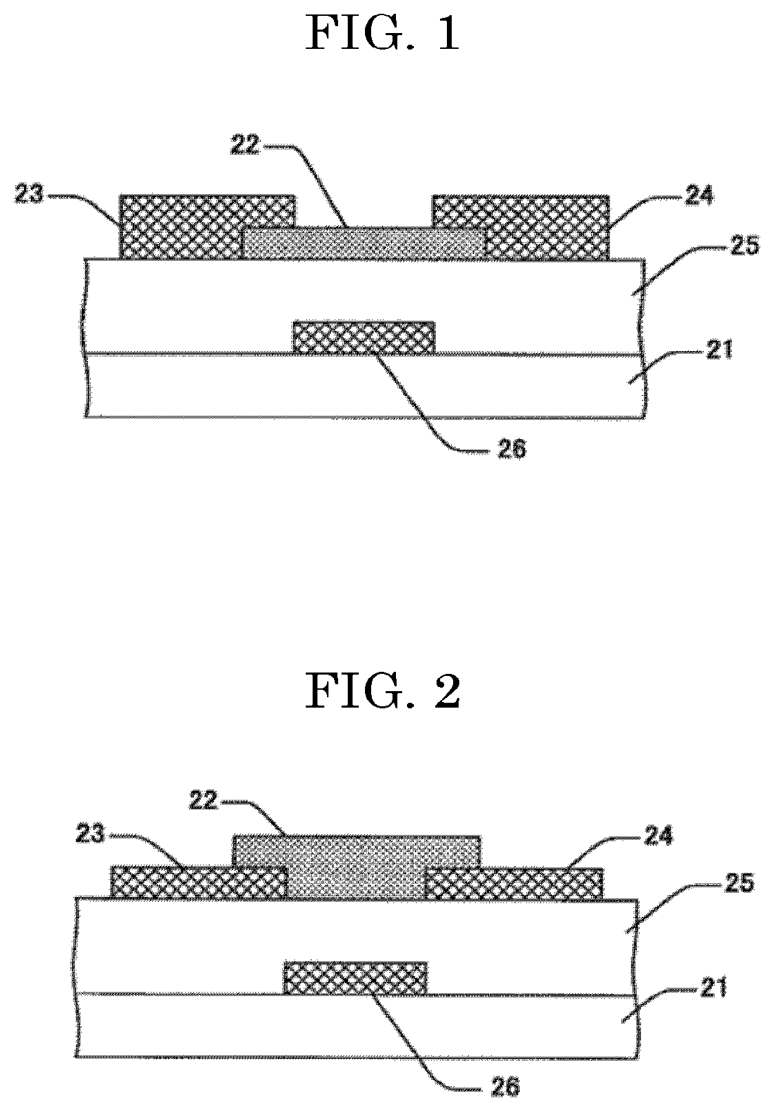
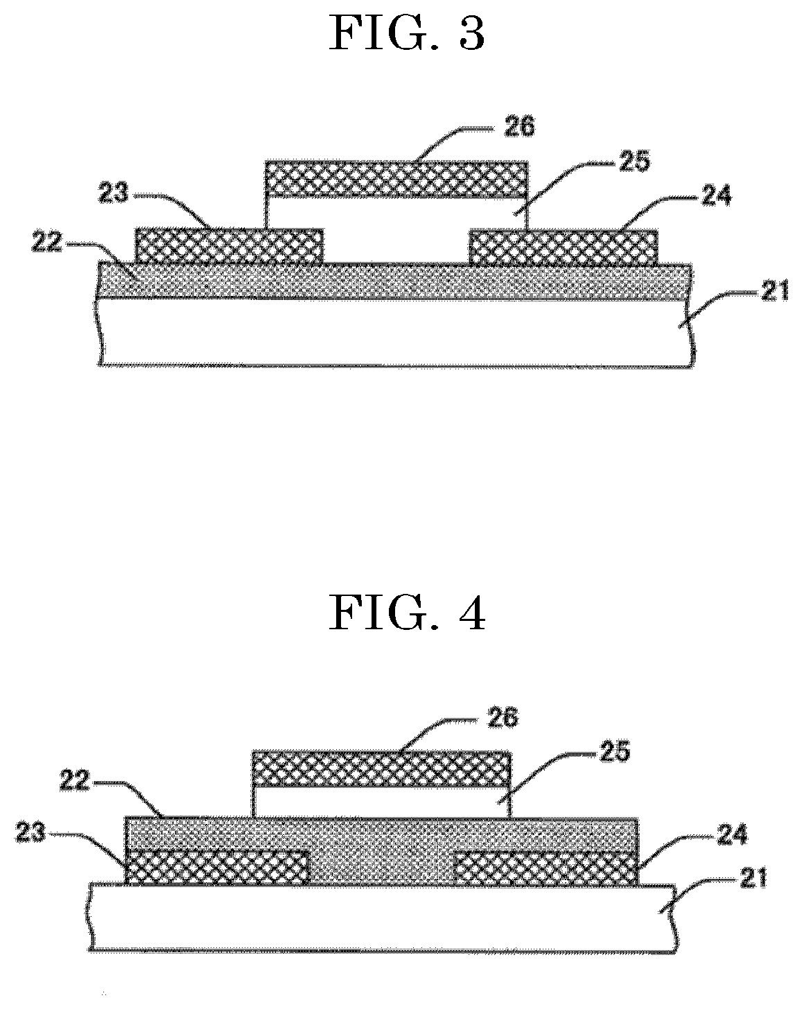
—Formation of Gate Electrode—

[0162]Al was vapor-deposited on a glass substrate so as to have a thickness of 100 nm and the resultant Al film was subjected to patterning into lines by photolithography and etching, to form a gate electrode.

—Formation of Gate Insulating Film—

[0163]Next, a film of SiON having a thickness of 200 nm was formed through plasma CVD using SiH4 gas and N2O gas as raw materials at a temperature of 200° C. The resultant film was used as a gate insulating film.

—Formation of Semiconductor Layer—

[0164]A film of In2O3 doped with Sn was formed on the gate insulating film through RF magnetron sputtering so as to have a film thickness of 20 nm. The target used was a polycrystalline sintered body having a composition of In1.96Sn0.04O3. Argon gas and oxygen gas were introduced as sputtering gas. The total pressure was fixed to 1.1 Pa and the oxygen concentration was set to 50% by volume. Patterning was performed through film formation via a metal mask. In the obtained se...


PUM

PropertyMeasurementUnit
thicknessaaaaaaaaaa
thicknessaaaaaaaaaa
thicknessaaaaaaaaaa

Abstract

A field-effect transistor including a semiconductor layer formed of an n-type metal oxide semiconductor, wherein the n-type metal oxide semiconductor includes indium oxide, wherein the indium oxide is n-type doped through introduction of one or more kinds of cations as dopants, and wherein the n-type metal oxide semiconductor has a peak detected at an angle corresponding to a (222) plane of indium oxide having a bixbite structure in an X-ray diffraction method using a two-dimensional detector.

Description

CROSS-REFERENCE TO RELATED APPLICATIONS[0001]The present application claims priority under 35 U.S.C. § 119 to Japanese Patent Application No. 2019-053473, filed Mar. 20, 2019. The contents of which are incorporated herein by reference in their entirety.BACKGROUND OF THE INVENTIONField of the Invention[0002]The present disclosure relates to a field-effect transistor, a display element, an image display device, and a system.Description of the Related Art[0003]Liquid crystal displays (LCDs), organic electroluminescence (EL) displays (OLEDs), and flat panel displays (FPDs) such as electronic paper are driven by driving circuits including thin-film transistors (TFTs) that use amorphous silicon or polycrystalline silicon in active layers thereof. FPDs have further been demanded to be larger in size, higher in definition, and faster in driving properties. This tendency demands TFTs having higher carrier mobility and more stable properties.[0004]However, there are both advantages and disadv...

Claims


Application Information

Patent Timeline
Patent Type & Authority Applications(United States)
IPC IPC(8): H01L29/786H01L27/12H01L29/24G09G3/30G09G3/36
CPCG09G3/36G02F1/167G02F1/13306G02F1/163G02B26/005H01L27/3262H01L27/1225G09G3/30G02F1/1685H01L29/78693H01L29/247H01L29/7869H01L29/66969H10K59/12G09G3/3648G09G3/3233G02B27/026H10K59/1213
Inventor ABE, YUKIKOANDO, YUICHINAKAMURA, YUKIMATSUMOTO, SHINJISONE, YUJIUEDA, NAOYUKISAOTOME, RYOICHIARAE, SADANORIKUSAYANAGI, MINEHIDE
Owner RICOH KK
Why Eureka
Try Eureka