Photoelectric conversion module and method for manufacturing photoelectric conversion module

Inactive Publication Date: 2021-01-28
IDEMITSU KOSAN CO LTD
View PDF0 Cites 0 Cited by
  • Summary
  • Abstract
  • Description
  • Claims
  • Application Information

AI Technical Summary

Benefits of technology

[0007]A photoelectric conversion module according to one aspect comprises: a photoelectric conversion cell including a first electrode layer, a second electrode layer, and a photoelectric conversion layer between the first electrode layer and the second electrode layer; and a plurality of grid electrodes arrayed in a first direction in the photoelectric conversion cell, the plurality of grid electrodes extending in a direction intersecting the first direction, wherein at least one of the first electrode layer and the second electrode layer is a transparent electrode layer, the transparent electrode layer includes a first region and a second region, the second region has sheet resistance smaller than sheet resistance in the first region, a film thickness larger than a film thickness in the first region, or transmittance smaller than transmittance in the first region, and an interval between the grid electrodes adjacent to each other in the first direction in the first region is smaller than an interval between the grid electrodes adjacent to each other in the fi

Problems solved by technology

Therefore, when a current generated by the photoelectric conversion flows through the transparent electrode layer, a power loss occurs due to the electric resistance v

Method used


Image

  • Photoelectric conversion module and method for manufacturing photoelectric conversion module
  • Photoelectric conversion module and method for manufacturing photoelectric conversion module
  • Photoelectric conversion module and method for manufacturing photoelectric conversion module

Examples


first embodiment

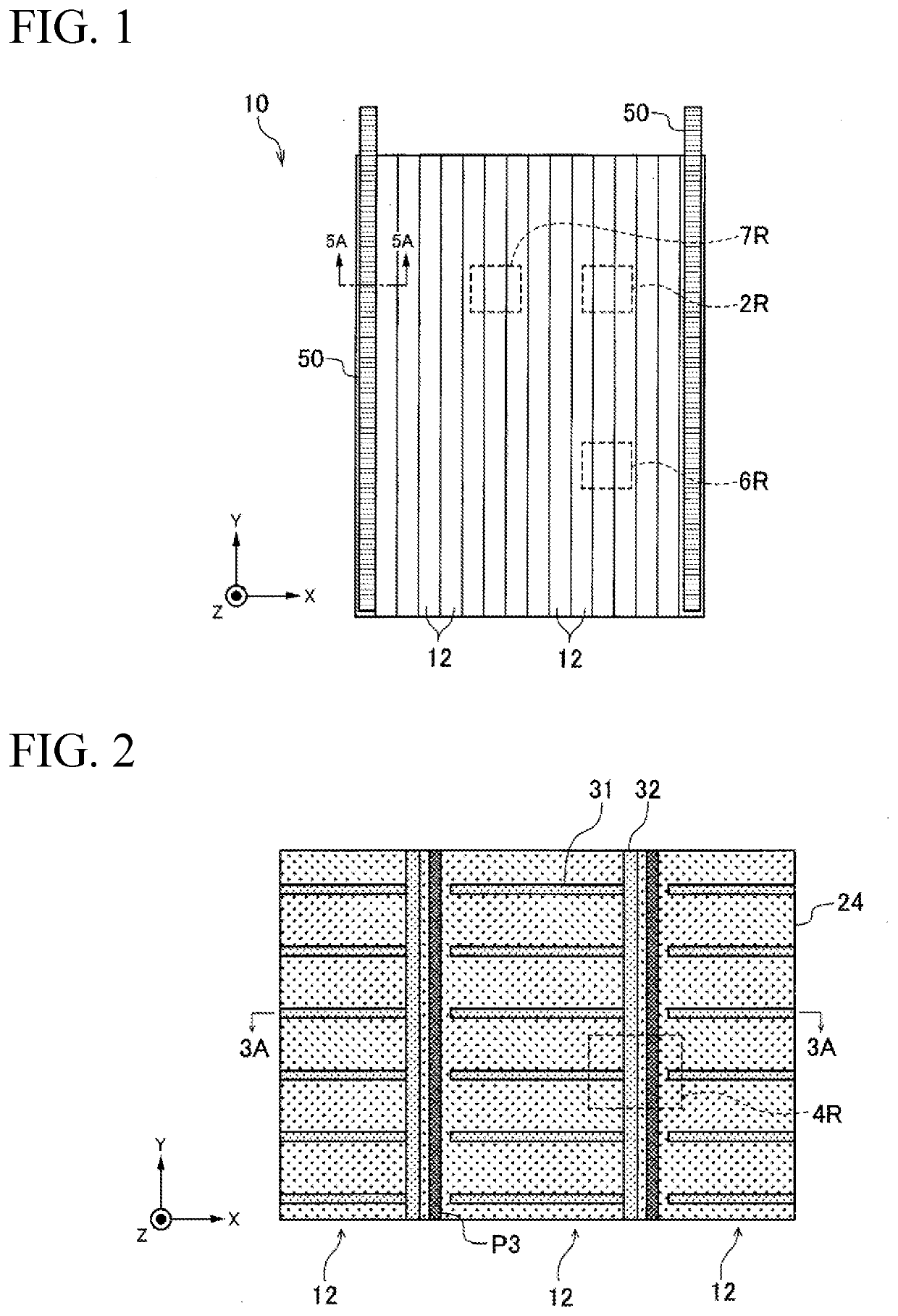
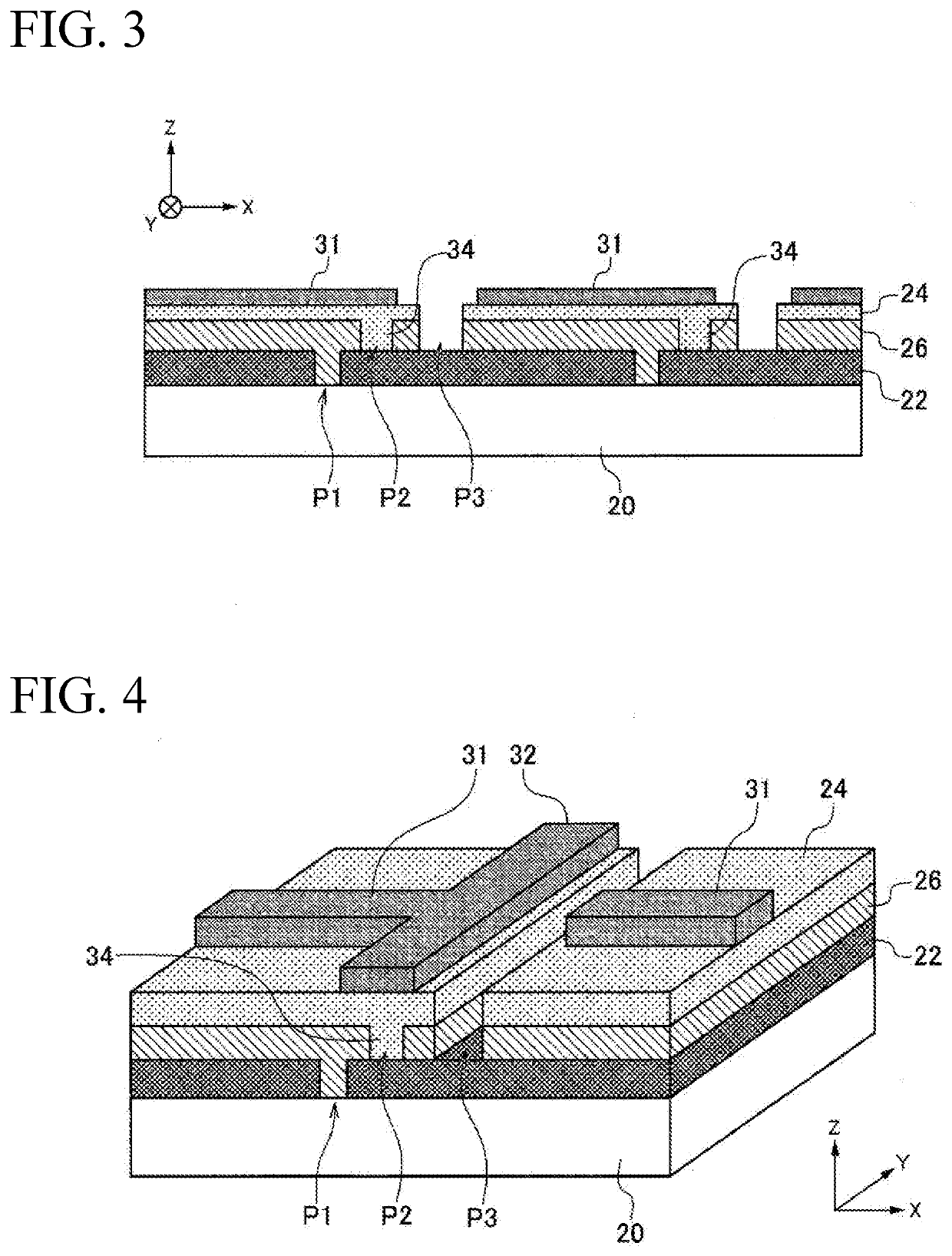
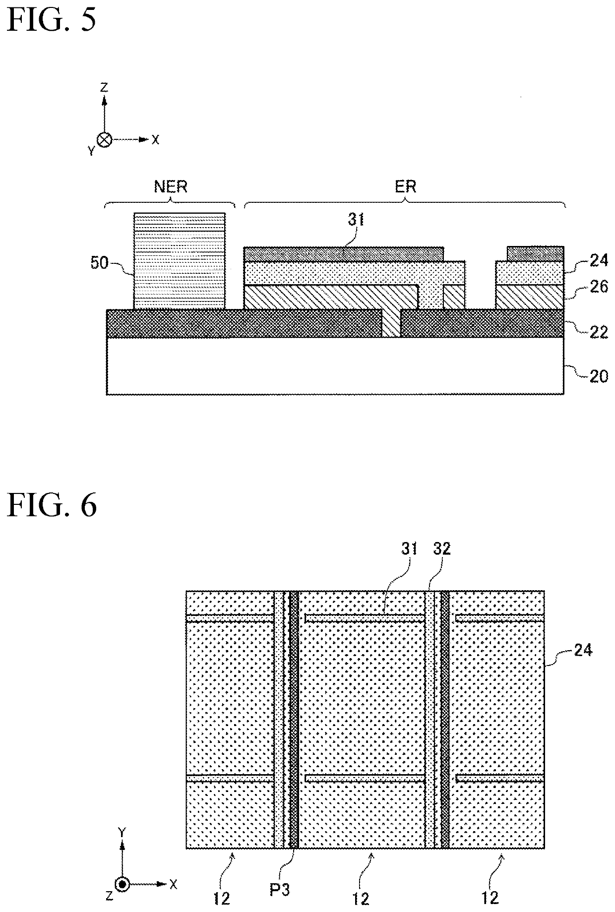
[0026]FIG. 1 is a schematic top view of a photoelectric conversion module according to a first embodiment. FIG. 2 is a schematic top view of the photoelectric conversion module in a region 2R in FIG. 1. FIG. 3 is a schematic cross-sectional view of the photoelectric conversion module taken along line 3A-3A in FIG. 2. FIG. 4 is a schematic perspective view of the photoelectric conversion module in a region 4R in FIG. 2. FIG. 5 is a schematic cross-sectional view of the photoelectric conversion module taken along line 5A-5A in FIG. 1FIG. 6 is a schematic top view of the photoelectric conversion module in a region 6R in FIG. 1. FIG. 7 is a schematic top view of the photoelectric conversion module in a region 7R in FIG. 1.

[0027]A photoelectric conversion module 10 according to the present embodiment may be an integrated thin-film photoelectric conversion module including a plurality of photoelectric conversion cells 12 integrated on a substrate 20. Preferably, the photoelectric conversi...


PUM


Abstract

A photoelectric conversion module (10) comprises a photoelectric conversion cell (12) including a first electrode layer (22), a second electrode layer (24), and a photoelectric conversion layer (26); and a plurality of grid electrodes (31). At least one of the first electrode layer and the second electrode layer is a transparent electrode layer. The transparent electrode layer includes a first region and a second region. The second region has sheet resistance smaller than sheet resistance in the first region, a film thickness larger than a film thickness in the first region, or transmittance smaller than transmittance in the first region. An interval between the grid electrodes adjacent to each other in the first direction in the first region is smaller than an interval between the grid electrodes adjacent to each other in the first direction in the second region.

Description

TECHNICAL FIELD[0001]The present invention relates to a photoelectric conversion module having a grid electrode and a method for manufacturing the photoelectric conversion module.BACKGROUND ART[0002]A photoelectric conversion module such as a solar battery module including a plurality of photoelectric conversion cells is known (following Patent Literature 1). In an integrated thin-film photoelectric conversion module as described in Patent Literature 1, a photoelectric conversion cell includes a transparent electrode layer located on a light receiving surface, a rear surface electrode layer located on a surface opposite to the light receiving surface, and a photoelectric conversion layer between the transparent electrode layer and the rear surface electrode layer.[0003]An electric resistance value of the transparent electrode layer is generally higher than an electric resistance value of an opaque electrode layer made of metal. Therefore, when a current generated by the photoelectri...

Claims


Application Information

Patent Timeline
IPC IPC(8): H01L31/0224H01L31/18
CPCH01L31/022466H01L31/1884H01L31/0465H01L31/022433
Inventor YONEYAMA, NOBUTAKAHAMANO, MIKIOMIYAGAWA, YOSHIHIDEYAMAURA, TOSHIAKITANAKA, MANABUASANO, AKIHIKO
Owner IDEMITSU KOSAN CO LTD
Why Eureka
Try Eureka