Method of forming nanocluster-comprising dielectric layer and device comprising such layer

A dielectric layer, dielectric technology, applied in nanotechnology, nanotechnology, nanotechnology for information processing, etc., can solve the problems of troublesome and expensive manufacturing

Active Publication Date: 2014-05-14
TAIWAN SEMICON MFG CO LTD
View PDF4 Cites 0 Cited by
  • Summary
  • Abstract
  • Description
  • Claims
  • Application Information

AI Technical Summary

Problems solved by technology

While this nonvolatile memory cell includes improved charge trapping capabilities, it is cumbersome and expensive to manufacture

Method used


Image

  • Method of forming nanocluster-comprising dielectric layer and device comprising such layer
  • Method of forming nanocluster-comprising dielectric layer and device comprising such layer
  • Method of forming nanocluster-comprising dielectric layer and device comprising such layer

Examples


Embodiment Construction

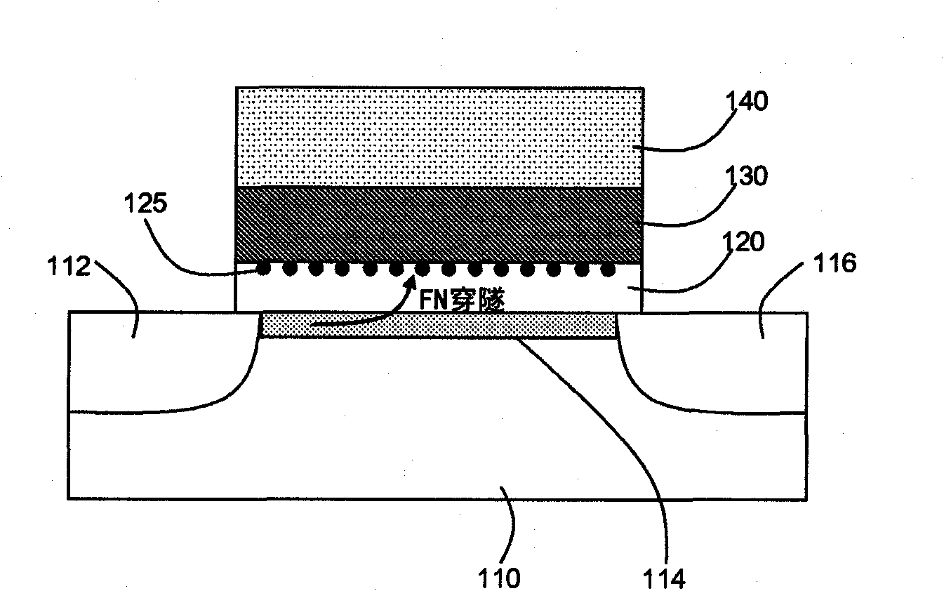
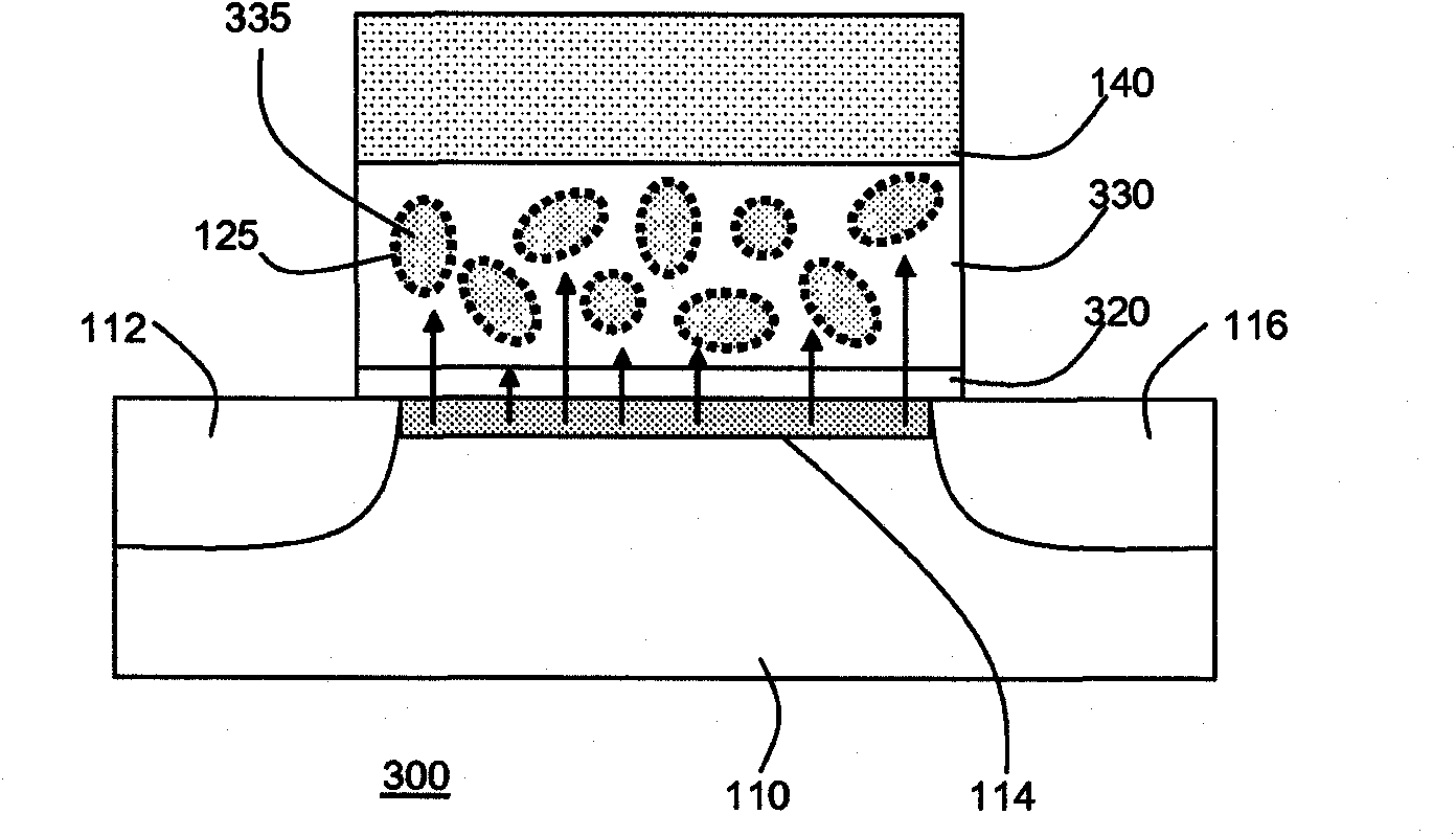
[0040] It should be understood that the drawings in the specification are schematic diagrams only and are not shown to scale. It should also be understood that in the drawings or descriptions in the specification, the same reference numerals are used for similar or identical parts.

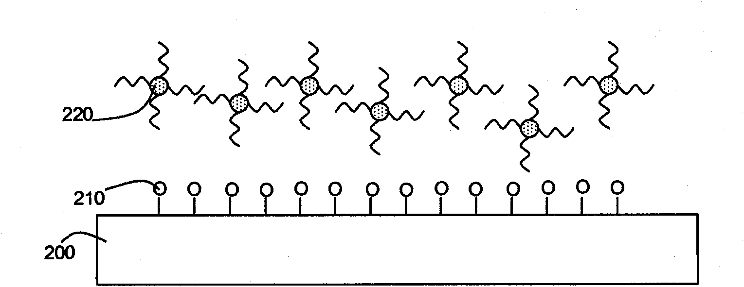
[0041] Figure 2a-Figure 2f A schematic diagram of forming a dielectric layer using an atomic layer deposition (ALD) process. exist Figure 2a Among them, a functional substrate 200 has a surface 210 with hydroxyl groups. A dielectric precursor material 220 comprising a reactive compound, such as a metal ion surrounded by organic ligands or other suitable substituents such as halides, is pulsed over the surface 210 of the functional substrate 200 .

[0042] Such as Figure 2b As shown, this will cause a chemical reaction therein, and the substituents removed from the dielectric precursor material 220 will be replaced by a bridge between the metal ions in the dielectric precursor material 220 a...


PUM


Abstract

A method of forming a dielectric layer on a further layer of a semiconductor device is disclosed. The method comprises depositing a dielectric precursor compound and a further precursor compound over the further layer, the dielectric precursor compound comprising a metal ion from the group consisting of Yttrium and the Lanthanide series elements, and the further precursor compound comprising a metal ion from the group consisting of group IV and group V metals; and chemically converting the dielectric precursor compound and the further precursor compound into a dielectric compound and a further compound respectively, the further compound self-assembling during said conversion into a plurality of nanocluster nuclei within the dielectric layer formed from the first dielectric precursor compound. The nanoclusters may be dielectric or metallic in nature. Consequently, a dielectric layer is formed that has excellent charge trapping capabilities. Such a dielectric layer is particularly suitable for use in semiconductor devices such as non-volatile memories.

Description

technical field [0001] The present invention relates to a method of forming a dielectric layer containing nanoclusters on an additional layer of a semiconductor device. [0002] In particular, the present invention relates to a semiconductor device comprising the above-mentioned dielectric layer. Background technique [0003] The continuous miniaturization of semiconductor components triggers the development of new materials and new designs of semiconductor components in order to overcome the problems related to the above-mentioned miniaturization of semiconductor components. For example, reducing the layer thickness of dielectric layers in semiconductor devices such as transistors and memory cells not only increases the switching speed of the device, but also increases leakage through the dielectric layer. To overcome the leakage problem, so-called high-k materials are used as dielectric layers. These materials have a dielectric constant substantially higher than that of ...

Claims


Application Information

Patent Timeline
Patent Type & Authority Patents(China)
IPC IPC(8): H01L21/28C23C14/08C23C16/40H01L21/314H01L29/423H01L29/51
CPCB82Y10/00H01L29/42332H01L21/28273H01L21/3141H01L29/7883C23C16/45531C23C16/30H01L29/792H01L21/28282H01L29/40114H01L29/40117H01L21/02192H01L21/02205H01L21/0228H01L29/51
Inventor 贾奈许·B·P·寇朱普瑞克温·贝斯林乔罕·H·克鲁托克罗伯图斯·A·M·沃尔特弗莱迪·卢兹本
Owner TAIWAN SEMICON MFG CO LTD
Why Eureka
Try Eureka