Method for accurately controlling steepness when silicon carbide high-temperature ions are injected into mask

A high-temperature ion implantation and precise control technology, applied in semiconductor/solid-state device manufacturing, electrical components, circuits, etc., can solve problems such as inaccessibility, deformation of photoresist, deformation of etching surface, etc., to improve breakdown characteristics, Easy to remove and avoid the effect of injecting dead ends

Active Publication Date: 2014-02-05
江苏中科汉韵半导体有限公司
View PDF6 Cites 7 Cited by
  • Summary
  • Abstract
  • Description
  • Claims
  • Application Information

AI Technical Summary

Problems solved by technology

In order to avoid pollution caused by metals, photoresist is generally used as the etch barrier layer of the dielectric mask, but the photoresist is easily deformed during the dry etching process, and the change of the etch barrier layer will cause damage to the etched surface. Deformation, unable to obtain ion implantation masks with steep sidewalls required in the fabrication of silicon carbide devices

Method used


Image

  • Method for accurately controlling steepness when silicon carbide high-temperature ions are injected into mask
  • Method for accurately controlling steepness when silicon carbide high-temperature ions are injected into mask

Examples


Embodiment

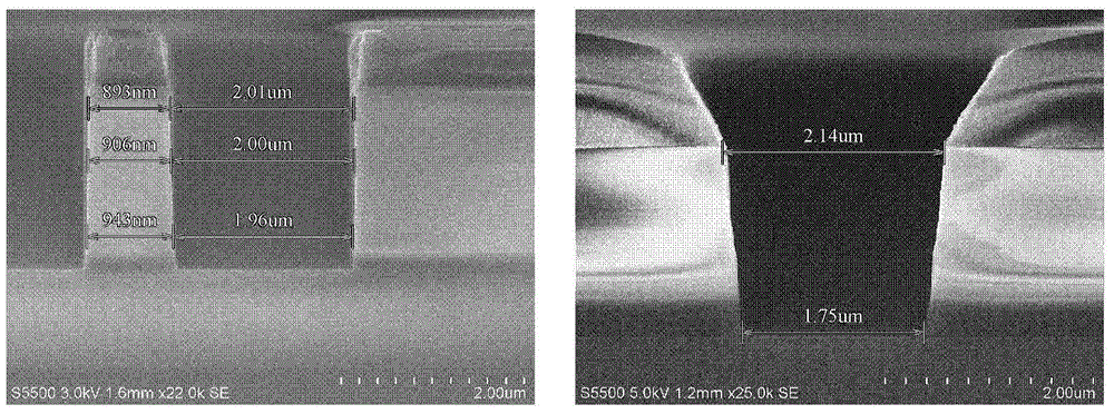
[0036] The present invention takes the method of precisely controlling the steepness of a silicon carbide high-temperature ion implantation mask on a silicon carbide epitaxial substrate as an example to describe the present invention in detail, and the specific process steps are as follows:

[0037]1) Use standard RCA to clean (3#, 1# each 10min) SiC epitaxial substrate, and use N 2 Blow dry chips.

[0038] 2) A PECVD growth method is adopted on the silicon carbide epitaxial substrate, and a 2 μm high-temperature ion implantation masking layer is grown at 270° C., and the growth rate is 1000 A / 3 min.

[0039] 3) On the high-temperature ion-implanted mask layer, a 500A amorphous silicon layer is grown at 550° C. by LPCVD method as an etching barrier layer, and the growth rate is 10-20 A / min.

[0040] 4) The uniform i-line photoresist is 1 μm, and the photoresist is exposed to 2000J / cm 2 , develop for 1 min, and obtain the selective ion implantation area window.

[0041] 5) U...


PUM


Abstract

The invention discloses a method for accurately controlling steepness when silicon carbide high-temperature ions are injected into a mask. The method comprises the steps that a silicon carbide epitaxial substrate is cleaned; a high-temperature ion injection masking layer capable of sufficiently resisting against the injected high-temperature and high-energy ions grows on the surface of the silicon carbide epitaxial substrate; an etching resisting layer used for controlling an etching process grows on the high-temperature ion injection masking layer; photoresist coats the etching resisting layer, and a selective high-temperature ion area window is formed in the surface of the etching resisting layer by adopting a photoetching developing technology, etching is sequentially carried out on the etching resisting layer and the high-temperature ion injection masking layer from the selective high-temperature ion area window to the surface of the silicon carbide epitaxial substrate; the photoresist and the unnecessary etching resisting layer are removed to obtain the steep and controllable thick-medium ion injection masking layer with the smooth lateral wall. By means of the method, angle control over an etching surface is carried out accurately, the steep thick-medium ion injection masking layer with the smooth lateral wall is obtained, and good uniformity and strong controllability of the selective ion injection area are guaranteed.

Description

technical field [0001] The invention relates to the fields of ion implantation mask preparation technology and etching / corrosion technology, in particular to a method for precisely controlling the steepness of a silicon carbide (SiC) high temperature ion implantation mask. Background technique [0002] Silicon carbide material has excellent physical and electrical properties. With its unique advantages such as wide band gap, high thermal conductivity, large saturation drift velocity and high critical breakdown electric field, it has become a high-power, high-frequency, durable It is an ideal semiconductor material for high-temperature and radiation-resistant devices, and has broad application prospects in military and civil affairs. Power electronic devices made of SiC materials have become one of the hot devices and frontier research fields in the field of semiconductors. [0003] Mask technology is one of the important processes in semiconductor manufacturing, and it is a...

Claims


Application Information

Patent Timeline
Patent Type & Authority Applications(China)
IPC IPC(8): H01L21/04H01L21/266
CPCH01L21/0465
Inventor 刘新宇汤益丹许恒宇蒋浩杰赵玉印申华军白云杨谦
Owner 江苏中科汉韵半导体有限公司
Why Eureka
Try Eureka