Groove power device with buried layer and manufacturing method thereof

A manufacturing method and technology of power devices, which are applied in semiconductor/solid-state device manufacturing, semiconductor devices, electrical components, etc., and can solve problems such as increased on-resistance

Inactive Publication Date: 2016-11-23
PEKING UNIV FOUNDER GRP CO LTD +1
View PDF4 Cites 3 Cited by
  • Summary
  • Abstract
  • Description
  • Claims
  • Application Information

AI Technical Summary

Problems solved by technology

The breakdown point of the trench power device is concentrated at the corner of the bottom of the trench. The reduction of the concentration and the increase of the depth of the

Method used


Image

  • Groove power device with buried layer and manufacturing method thereof
  • Groove power device with buried layer and manufacturing method thereof
  • Groove power device with buried layer and manufacturing method thereof

Examples


no. 1 example

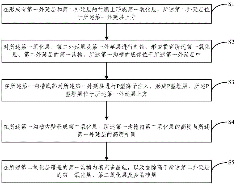
[0050] figure 1 The method for fabricating the buried trench power device provided by the first embodiment of the present invention is shown, as figure 1 As shown, the manufacturing method of the power device with a buried trench provided by the first embodiment of the present invention is as follows.

[0051] S1. Form a first oxide layer on a substrate formed with a first epitaxial layer and a second epitaxial layer, the second epitaxial layer is located above the first epitaxial layer.

[0052] In a specific application, the first epitaxial layer is an N-type epitaxial layer, and the second epitaxial layer is a P-type epitaxial layer.

[0053] In a specific application, the substrate of the present embodiment and / or the matrix of the first epitaxial layer and / or the second epitaxial layer may be single crystal silicon or the like.

[0054]S2. Etching the first oxide layer, the second epitaxial layer, and the first epitaxial layer to form a first trench penetrating through ...

no. 2 example

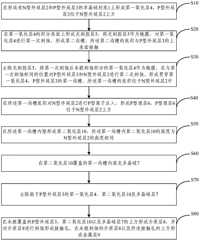
[0078] In order to more clearly illustrate the technical solutions of the embodiments of the present invention, a more specific embodiment is given below, figure 2 It shows a schematic flowchart of a method for fabricating a power device with a buried trench provided by the second embodiment of the present invention, as shown in figure 2 As shown, in this embodiment, single crystal silicon is used as the substrate, and the method for manufacturing a power device with a buried trench provided by the second embodiment of the present invention is as follows.

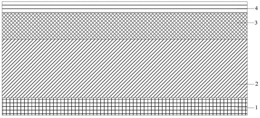
[0079] S10, forming a first oxide layer 4 on the single crystal silicon substrate 1 formed with an N-type epitaxial layer 2 and a P-type epitaxial layer 3, and the P-type epitaxial layer 3 is located above the N-type epitaxial layer 2, such as image 3 shown.

[0080] It should be noted that the selection of the substrate material mainly depends on the following aspects: structural properties, interface properties, chemi...

no. 3 example

[0095] This embodiment provides a power device with a buried trench, and the power device with a buried trench is manufactured using the manufacturing method described in the first or second embodiment.

[0096] In the trench power device with a buried layer in this embodiment, the P-type buried layer in the N-type drift region can increase the withstand voltage of the depletion layer of the trench power device, and can reduce the on-resistance of the device under the same withstand voltage. The second oxide layer can improve the withstand voltage capability at the corner at the bottom of the trench, and greatly improve the breakdown characteristics of the device.


PUM

PropertyMeasurementUnit
Thicknessaaaaaaaaaa

Abstract

The invention discloses a groove power device with a buried layer and a manufacturing method thereof. The manufacturing method comprises the steps that a first oxide layer is formed on a substrate on which a first epitaxial layer and a second epitaxial layer are formed, and the second epitaxial is arranged on the first epitaxial layer; the first oxide layer, the second epitaxial layer and the first epitaxial layer are etched so that a first groove which penetrates through the first oxide layer and the bottom part of the second epitaxial layer to be arranged in the first epitaxial layer is formed; P-type ion injection is performed on the first epitaxial layer at the bottom part of the first groove so that a P-type buried layer arranged on the first epitaxial layer is formed; a second oxide layer having the same height with the first epitaxial layer is formed on the internal wall of the first groove; and polycrystalline silicon is filled in the first groove covered by the second oxide layer, and the first and second oxide layers higher than the second epitaxial layer and the polycrystalline silicon layer are removed. According to the method, withstand voltage of the depletion layer of the groove power device can be enhanced, conduction resistance of the device can be reduced under the same withstand voltage, and the withstand voltage capacity of the bottom corner of the groove can be enhanced so that the breakdown properties of the device can be greatly improved.

Description

technical field [0001] The invention relates to the technical field of semiconductors, in particular to a trench power device with a buried layer and a manufacturing method thereof. Background technique [0002] Trench type Vertical Double Diffused Metal Oxide Semiconductor (VDMOS) transistors combine the advantages of bipolar transistors and ordinary Metal Oxide Semiconductor (MOS) devices, whether it is switching applications or linear applications , VDMOS is an ideal power device. The drain and source poles of VDMOS are on both sides of the device, so that the current flows vertically inside the device, which increases the current density and improves the rated current. The on-resistance per unit area is also small, which is A very versatile power device. [0003] In the design process of trench power devices, the contradiction between breakdown voltage and on-resistance is the bottleneck of device performance improvement. The breakdown point of the trench power device ...

Claims


Application Information

Patent Timeline
IPC IPC(8): H01L21/336H01L21/28H01L29/78H01L29/06H01L29/423
CPCH01L29/0623H01L29/42364H01L29/66712H01L29/7813H01L29/66734
Inventor 李理马万里赵圣哲
Owner PEKING UNIV FOUNDER GRP CO LTD
Why Eureka
Try Eureka