Nonvolatile storage element and analog circuit provided with same

Active Publication Date: 2020-09-17
ASAHI KASEI ELECTRONICS CO LTD
View PDF1 Cites 0 Cited by
  • Summary
  • Abstract
  • Description
  • Claims
  • Application Information

AI Technical Summary

Benefits of technology

The present invention is for a pair of nonvolatile storage elements and an analog circuit that use them. These elements have exceptional charge holding ability, which helps to keep electric characteristics stable. The technical effect of this invention is to provide a more reliable and accurate analog circuit that can operate consistently even in the absence of power.

Problems solved by technology

However, when the reference voltage variations in the reference voltage generation circuit are corrected by such a configuration, an increase in the layout area of the reference voltage generation circuit or an increase in man-hour and manufacturing steps for voltage adjustment poses a problem.

Method used


Image

  • Nonvolatile storage element and analog circuit provided with same
  • Nonvolatile storage element and analog circuit provided with same
  • Nonvolatile storage element and analog circuit provided with same

Examples


first embodiment

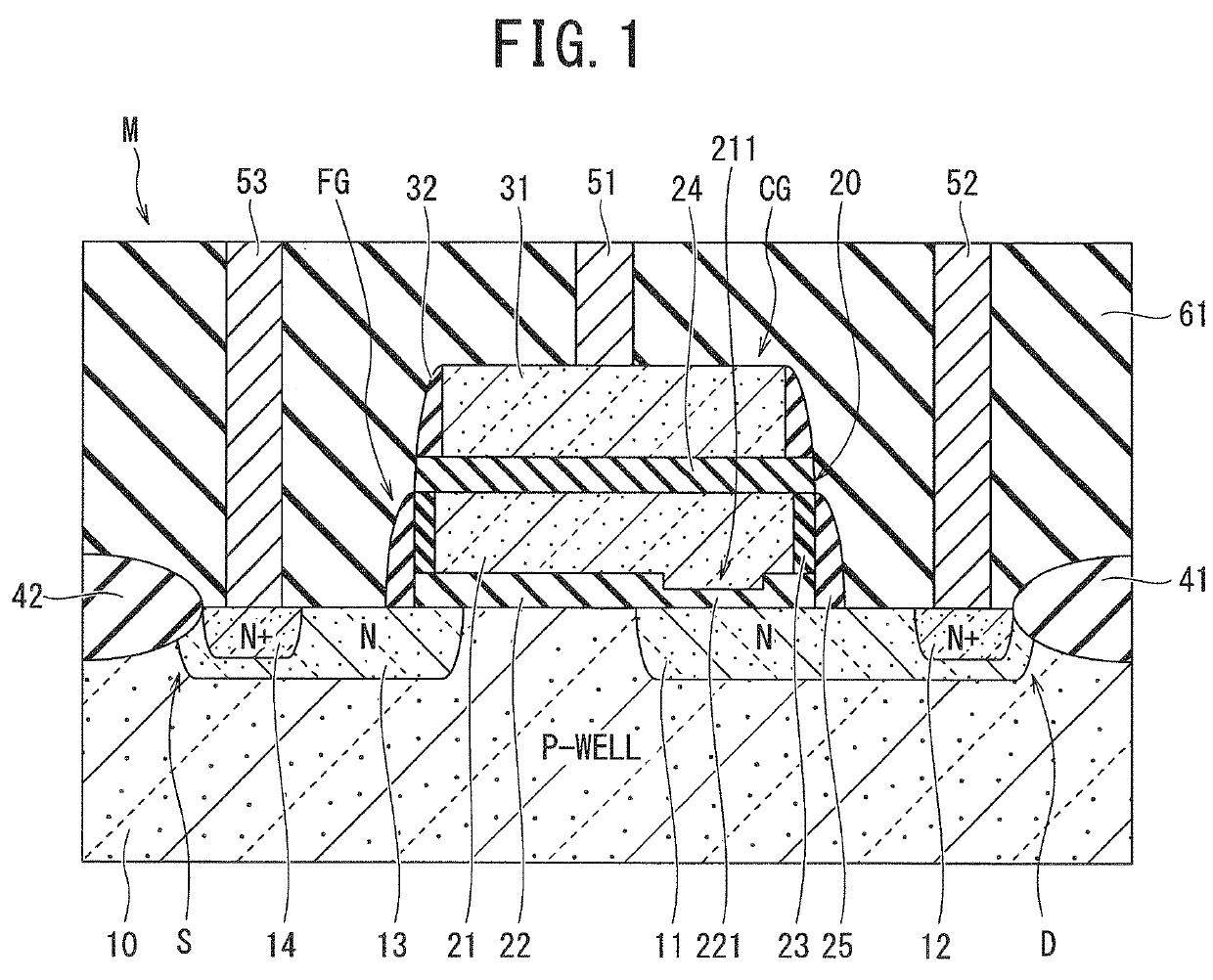
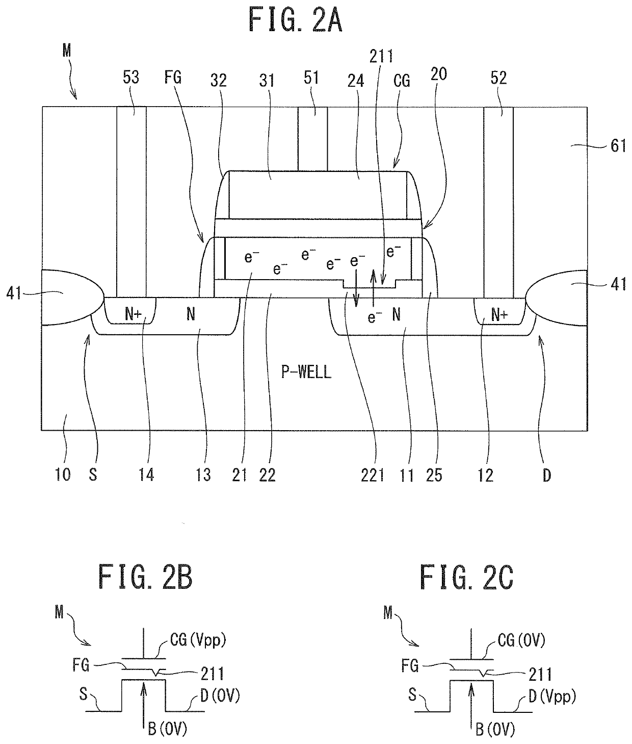
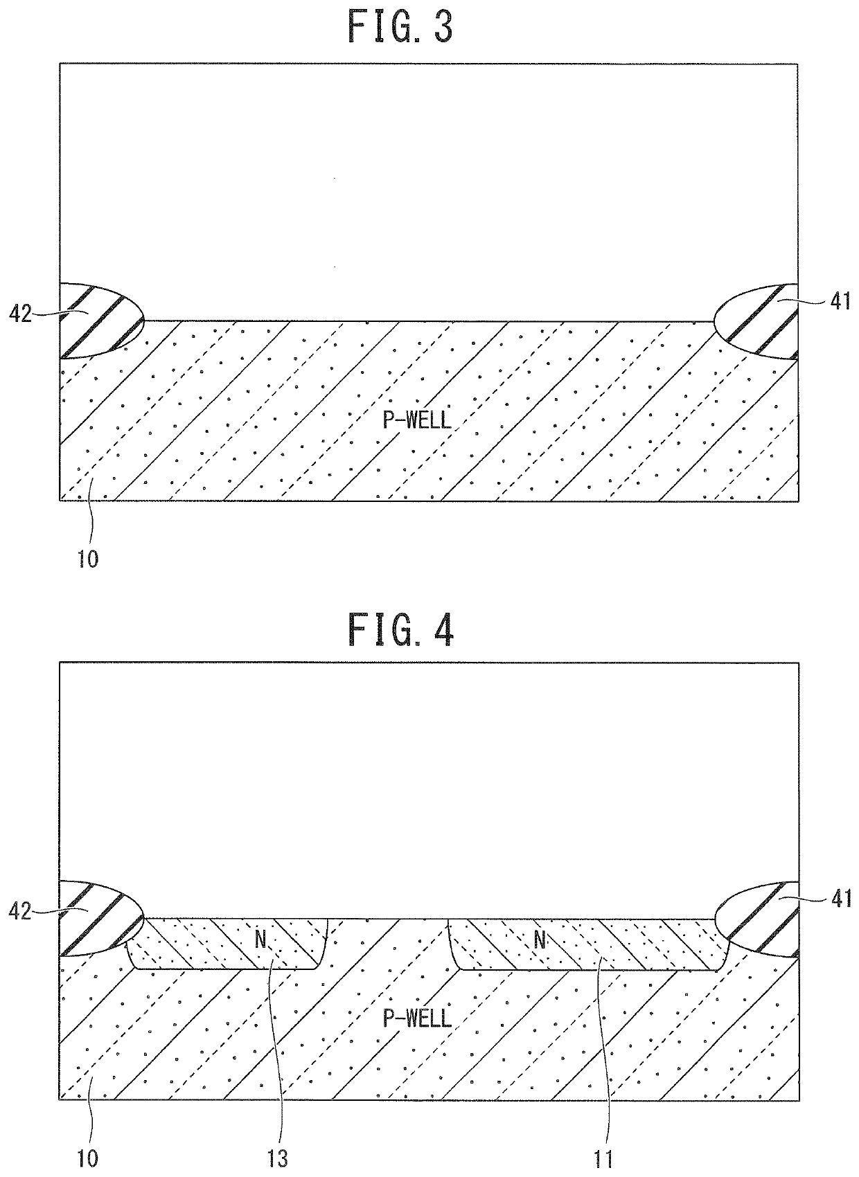
[0043]A nonvolatile storage element and an analog circuit provided with the same according to a first embodiment of the present invention are described using FIGS. 1 to 17. This embodiment describes a reference voltage generation circuit using an N-type nonvolatile storage element provided with a floating gate region having an insulator containing fluoride in the periphery thereof and a control gate region as an example of the analog circuit. However, when the nonvolatile storage element is not limited to the structure and is not limited to an N-type MOSFET insofar as the nonvolatile storage element is an active element (transistor) having a charge holding region. Furthermore, the analog circuit to which the nonvolatile storage element is applied is not limited to the reference voltage generation circuit insofar as the analog circuit is a circuit using the nonvolatile storage element in an analog manner. For example, the nonvolatile storage element is effective also in analog circui...

second embodiment

[0122]A nonvolatile storage element according to this embodiment and an analog circuit provided with the same according to a second embodiment of the present invention is described using FIGS. 18 to 22. A nonvolatile storage element according to this embodiment has a configuration in which the nonvolatile storage element M illustrated in FIG. 1 and a nonvolatile storage element Mr illustrated in FIG. 18 are contained as one set, floating gate regions of the nonvolatile storage element M and the nonvolatile storage element Mr are connected, and control gate regions of the nonvolatile storage element M and the nonvolatile storage element Mr are connected.

[0123]As illustrated in FIG. 18, the nonvolatile storage element Mr has the same configuration as that of the nonvolatile storage element M except that no charge inlet is provided. The nonvolatile storage element Mr is provided with a charge holding region 71 and an insulator 70 disposed surrounding the charge holding region 71 and ha...


PUM


Abstract

There is provided a nonvolatile storage element having excellent charge holding characteristics capable of reducing variations in electric characteristics and an analog circuit provided with the same. A nonvolatile storage element is provided with a charge holding region and an insulator surrounding the entire surface of the charge holding region and having halogen distributed in at least one part of a region surrounding the entire surface.

Description

TECHNICAL FIELD[0001]The present invention relates to a nonvolatile storage element and an analog circuit provided with the same.BACKGROUND ART[0002]In general, in a semiconductor device containing a reference voltage generation circuit, a reference voltage Vref assumed at the time of designing does not become a desired value and greatly varies in some cases due to manufacturing variations in a threshold voltage Vth of each transistor and a resistance value of a resistive element, and the like configuring the reference voltage generation circuit. Therefore, a highly accurate reference voltage generation circuit has been demanded in the semiconductor device requiring a stable reference voltage Vref. The semiconductor device is configured so that, in order to correct the reference voltage variations in the reference voltage generation circuit resulting from the manufacturing variations a large number of spare transistors adjusting the reference voltage by altering a wiring layer are b...

Claims


Application Information

Patent Timeline
IPC IPC(8): H01L29/788H01L27/11521H01L29/423H01L21/28H01L29/66
CPCH01L29/40114H01L29/42324H01L29/66825H01L27/11521H01L29/7883G11C16/0416G11C16/0408H10B41/30
Inventor SAKAMOTO, TOSHIROTAKEHARA, SATOSHIYAMAHA, YOSHIROKOBAYASHI
Owner ASAHI KASEI ELECTRONICS CO LTD
Why Eureka
Try Eureka