
Method of fabricating flash memory device

a technology of flash memory and fabricated materials, which is applied in the direction of semiconductor devices, basic electric elements, electrical equipment, etc., can solve the problems of degrading the electrical characteristics of the device, reducing the capacitance value of the dielectric film, etc., and achieve the effect of improving the charge retention characteristics of the flash memory devi

Inactive Publication Date: 2006-09-14
SK HYNIX INC
View PDF7 Cites 1 Cited by
  • Summary
  • Abstract
  • Description
  • Claims
  • Application Information

AI Technical Summary

Benefits of technology

[0010] A method of fabricating a flash memory device is disclosed which can improve charge retention characteristics of the flash memory device and prevent a smiling phenomenon of a tunnel oxide film and a dielectric film, which are generated after a thermal treatment process of a source / drain region.

Problems solved by technology

A capacitance value of the dielectric film also decreases due to the reduced cell ratio, which degrades the electrical characteristics of the device.

Method used


Image

  • Method of fabricating flash memory device
  • Method of fabricating flash memory device

Examples


Embodiment Construction

[0024] Where it is described below that one film is “on” the other film or a semiconductor substrate, the one film may directly contact the other film or the semiconductor substrate. Or, one or more films may be disposed between the one film and the other film or the semiconductor substrate. Furthermore, in the drawing, the thickness and size of each layer are not to scale and may be exaggerated for convenience of explanation and clarity. Like reference numerals are used to identify the same or similar parts.

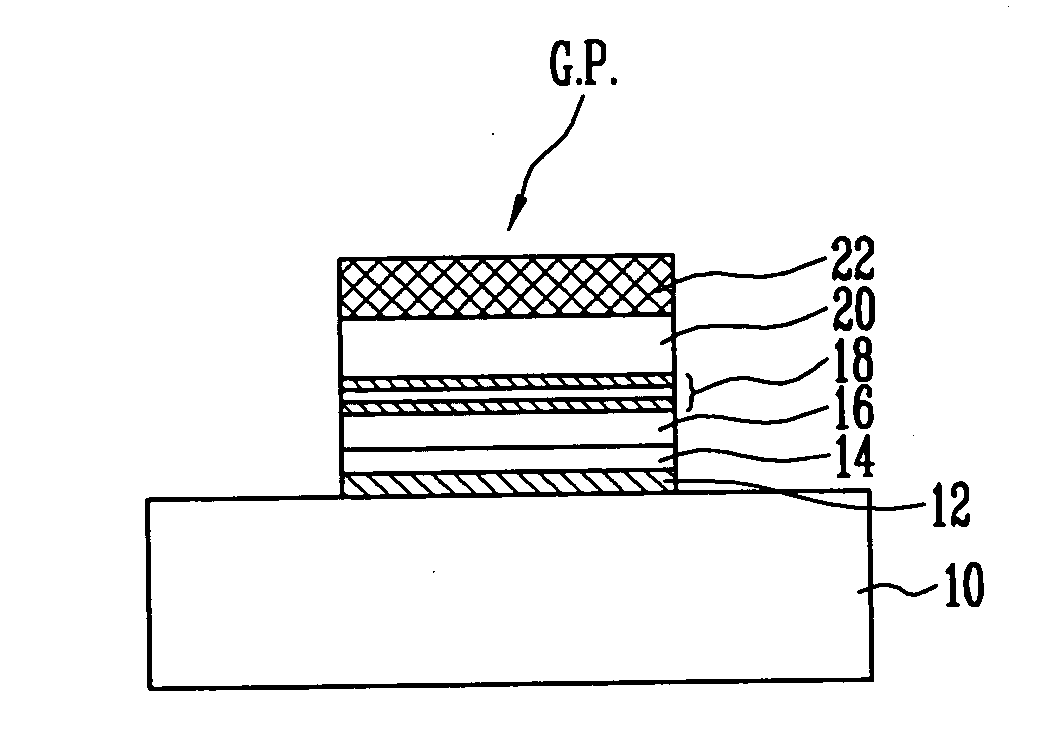
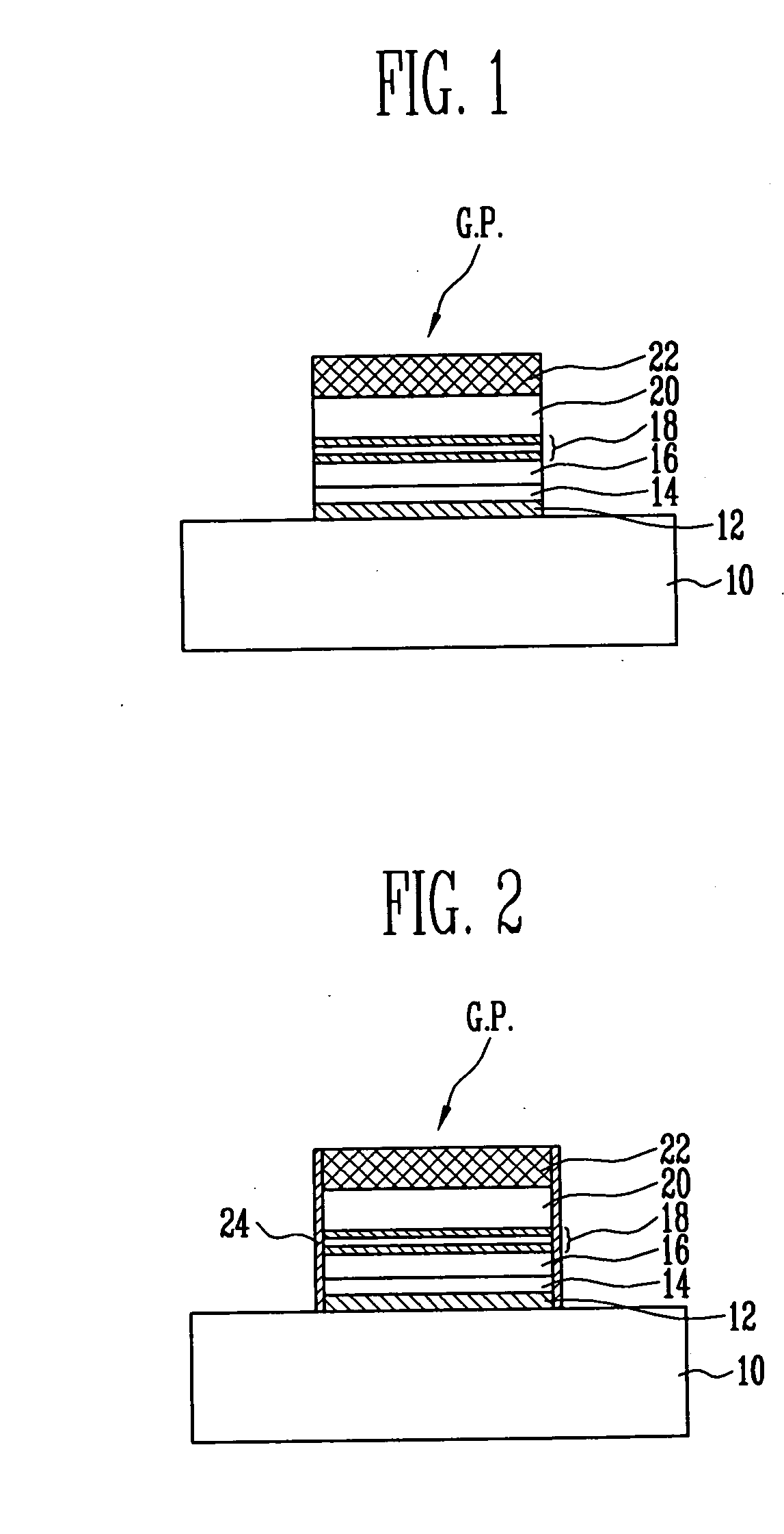
[0025]FIGS. 1 and 2 are cross-sectional views for explaining a disclosed method of fabricating a flash memory device.

[0026] Referring to FIG. 1, a tunnel oxide film 12 and a first polysilicon film 14 for floating gate electrode are sequentially formed on a semiconductor substrate 10.

[0027] At this time, the semiconductor substrate 10 is divided into a PMOS region and a NMOS region. A well region (not shown) and a region (not shown) into which an ion for threshold voltage cont...


PUM

PropertyMeasurementUnit
pressureaaaaaaaaaa
temperatureaaaaaaaaaa
pressureaaaaaaaaaa

Abstract

A method of fabricating a flash memory device is disclosed which includes sequentially stacking a tunnel oxide film, a first conductive film, a dielectric film, a second conductive film and a metal silicide film on a semiconductor substrate, and patterning the metal silicide film, the second conductive film, the dielectric film, the first conductive film and the tunnel oxide film to form a stack gate electrode, performing a radical oxidization process on the entire resulting surface having the stack gate electrode, whereby the profile of the stack gate electrode before the radical oxidization process is performed is maintained while forming a sidewall oxide film on sidewalls of the stack gate electrode, and performing a thermal treatment process of a hydrogen atmosphere on the entire resulting surface on which the radical oxidization process is performed.

Description

BACKGROUND [0001] 1. Technical Field [0002] Methods of fabricating flash memory devices are disclosed which result in improved charge retention characteristics and which avoid damage to the tunnel oxide and dielectric films during heat treatment of the source / drain region. [0003] 2. Discussion of Related Art [0004] During the fabrication of a flash memory device, a stack gate is formed on a semiconductor substrate, and a re-oxidization process is then performed. [0005] The re-oxidization process is performed to compensate for lateral damage of a tunnel oxide film during an etch process for forming a stack gate electrode pattern, and damage to a semiconductor substrate, which also happens during an etch process. A re-oxidization process can serve to mitigate damage of a semiconductor substrate to some degree when performing an ion implant process for forming source and drain regions, which is a subsequent process. [0006] Furthermore, a re-oxidization process may be performed to impro...

Claims


Application Information

Patent Timeline
Patent Type & Authority Applications(United States)
IPC IPC(8): H01L21/336
CPCH01L21/28247H01L21/28273H01L29/513H01L29/7881H01L29/40114H10B99/00
Inventor LEE, SEUNG CHEOLSONG, PIL GEUN
Owner SK HYNIX INC
Learn More