Memory cell with reduced DIBL and Vss resistance

a memory cell and dibl technology, applied in the field of semiconductor fabrication, can solve the problems of short channel effect known as drain induced barrier lowering (dibl), undesired reduction of effective channel length, detrimental to memory cell performance, etc., to reduce reduce drain induced barrier lowering, the effect of reducing lateral straggle and diffusion

Active Publication Date: 2007-01-30
MONTEREY RES LLC
View PDF8 Cites 8 Cited by
  • Summary
  • Abstract
  • Description
  • Claims
  • Application Information

AI Technical Summary

Benefits of technology

[0007]According to this exemplary embodiment, the spacer causes the source to have a reduced lateral straggle and diffusion in the channel region. The reduced lateral straggle and diffusion of the source in the channel region causes a reduction in drain induced barrier lowering (DIBL) in the floating gate memory cell. The method further comprises forming a Vss connection region under the bottom of the recess and under the source, where the Vss connection region is connected to the source. The recess allows a resistance of the Vss connection region to be decreased without increasing DIBL in the floating gate memory cell. Other features and advantages of the present invention will become more readily apparent to those of ordinary skill in the art after reviewing the following detailed description and accompanying drawings.

Problems solved by technology

However, by introducing the amount and depth of doping required to sufficiently lower Vss resistance, the effective channel length can be undesirably reduced.
As a result, a short channel effect known as drain induced barrier lowering (DIBL) can undesirably increase in a flash memory cell, such as a floating gate flash memory cell.
As a result of DIBL, the memory cell's threshold voltage decreases, which detrimentally affects memory cell performance.

Method used


Image

  • Memory cell with reduced DIBL and Vss resistance
  • Memory cell with reduced DIBL and Vss resistance
  • Memory cell with reduced DIBL and Vss resistance

Examples


Embodiment Construction

[0017]The present invention is directed to a memory cell with reduced DIBL and Vss resistance. The following description contains specific information pertaining to the implementation of the present invention. One skilled in the art will recognize that the present invention may be implemented in a manner different from that specifically discussed in the present application. Moreover, some of the specific details of the invention are not discussed in order not to obscure the invention.

[0018]The drawings in the present application and their accompanying detailed description are directed to merely exemplary embodiments of the invention. To maintain brevity, other embodiments of the present invention are not specifically described in the present application and are not specifically illustrated by the present drawings.

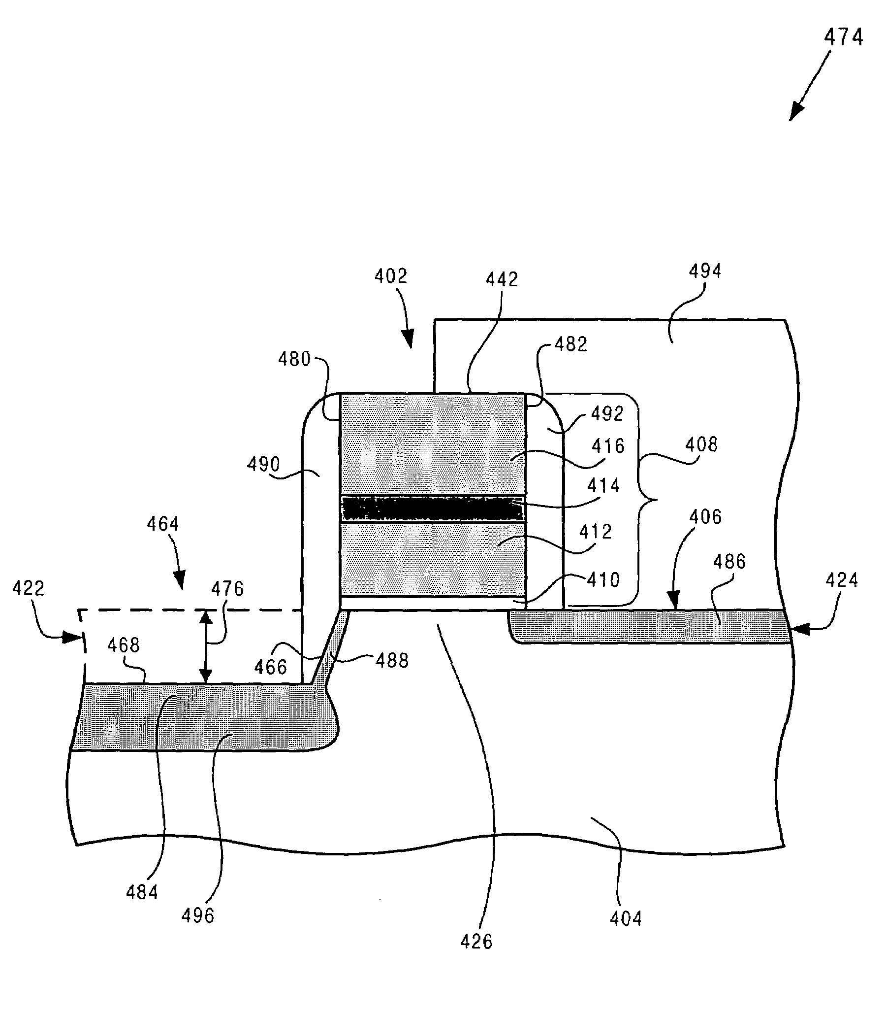
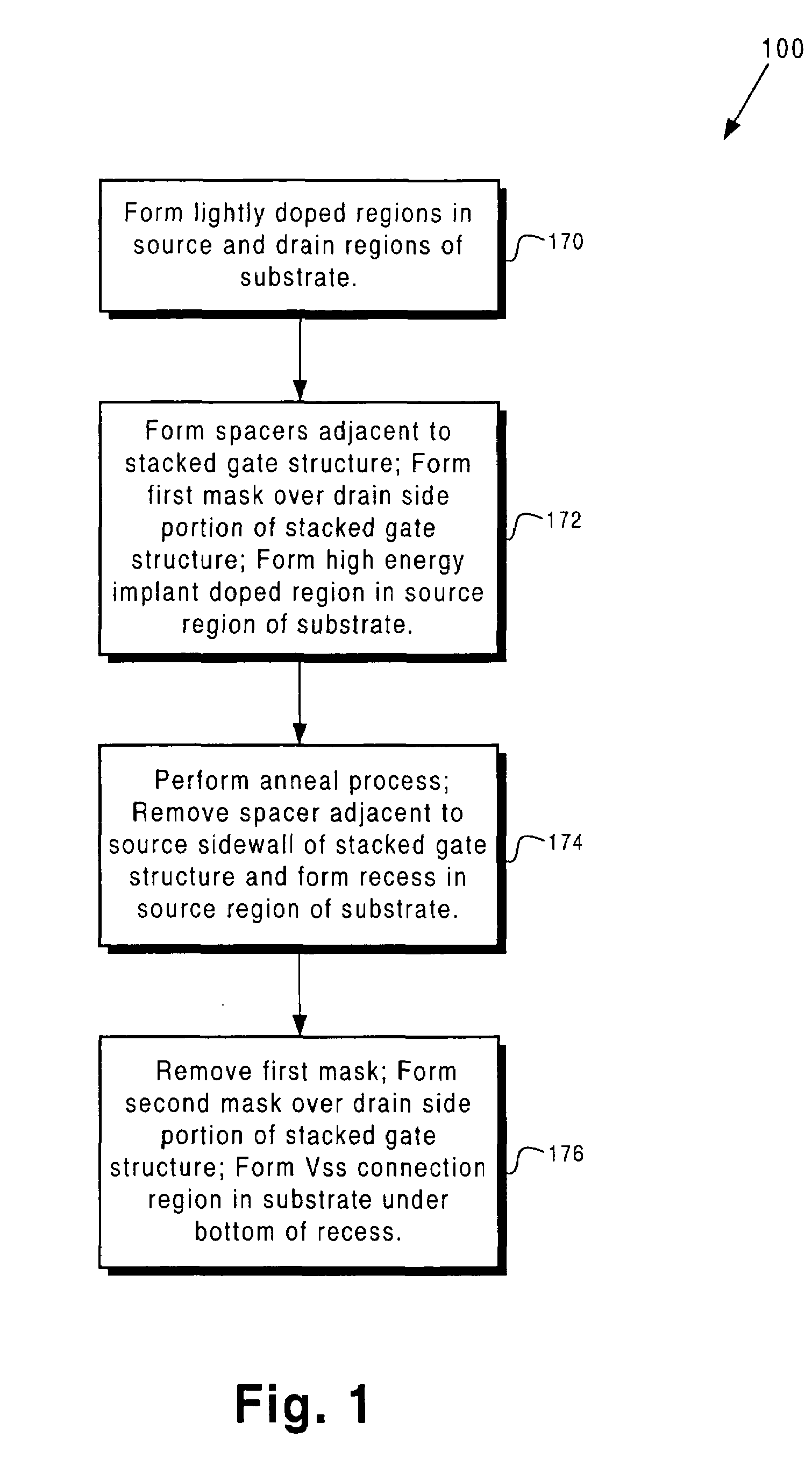
[0019]FIG. 1 shows a flowchart illustrating an exemplary method for forming a floating gate flash memory cell including a recessed Vss implant region and a source having re...


PUM


Abstract

According to one exemplary embodiment, a method for fabricating a floating gate memory cell on substrate comprises a step of forming a spacer adjacent to a source sidewall of a stacked gate structure, where the stacked gate structure is situated over a channel region in substrate. The method further comprises forming a high energy implant doped region adjacent to the spacer in the source region of substrate. The method further comprises forming a recess in a source region of the substrate, where the recess has a sidewall, a bottom, and a depth, and where the sidewall of the recess is situated adjacent to a source of the floating gate memory cell. According to this exemplary embodiment, the spacer causes the source to have a reduced lateral straggle and diffusion in the channel region, which causes a reduction in drain induced barrier lowering (DIBL) in the floating gate memory cell.

Description

TECHNICAL FIELD[0001]The present invention is generally in the field of semiconductor fabrication. More particularly, the present invention is in the field of floating gate memory device fabrication.BACKGROUND ART[0002]High performance flash memory devices, such as NOR-type flash memory devices, require high density and high operating speed as the device dimensions are scaled down. A low resistance Vss line, which connects source regions of flash memory cells situated between word lines, is used to reduce memory core cell size, improve circuit density, and increase flash memory device performance.[0003]In a conventional flash memory process flow, the Vss line can be formed by heavily doping the semiconductor substrate by using a Vss connection implant. In order to achieve a desirably low Vss resistance, a sufficient amount and a sufficient depth of doping are required along the Vss line in the semiconductor substrate. However, by introducing the amount and depth of doping required t...

Claims


Application Information

Patent Timeline
Patent Type & Authority Patents(United States)
IPC IPC(8): H01L29/788H01L21/336
CPCH01L29/66825H01L21/18
Inventor FANG, SHENQINGCHANG, KUO-TUNGFASTENKO, PAVELWANG, ZHIGANG
Owner MONTEREY RES LLC
Why Eureka
Try Eureka