Controlled substrate voltage for memory switches

a technology of memory switches and substrate voltages, which is applied in the direction of digital storage, instruments, computing, etc., can solve the problems of reducing device performance, increasing source to substrate voltage, and increasing threshold voltag

Inactive Publication Date: 2007-01-30
POLARIS INNOVATIONS LTD
View PDF6 Cites 9 Cited by
  • Summary
  • Abstract
  • Description
  • Claims
  • Application Information

AI Technical Summary

Benefits of technology

[0011]The present invention provides a solution that can reduce the increase in the threshold voltage of dynamic random access memory (“DRAM”) devices, thereby improving device performance during operation. The use of body contacts as described herein can provide variable substrate voltages during DRAM operation. The body contacts can change the body bias of activated memory cells, while maintaining the body bias of inactive memory cells. This can reduce the body effect (i.e., variation of the threshold voltage due to a variation of the substrate or bulk voltage) and can therefore provide improved array device performance (e.g., reduced data corruption) while the word line (“WL”) is activated.

Problems solved by technology

However, this can result in increased source to substrate voltages, thereby increasing the threshold voltage and reducing device performance (e.g., reduced write back current).
Additionally, DRAM devices may not share a common substrate, but may have individual substrate wells.

Method used


Image

  • Controlled substrate voltage for memory switches
  • Controlled substrate voltage for memory switches
  • Controlled substrate voltage for memory switches

Examples


Embodiment Construction

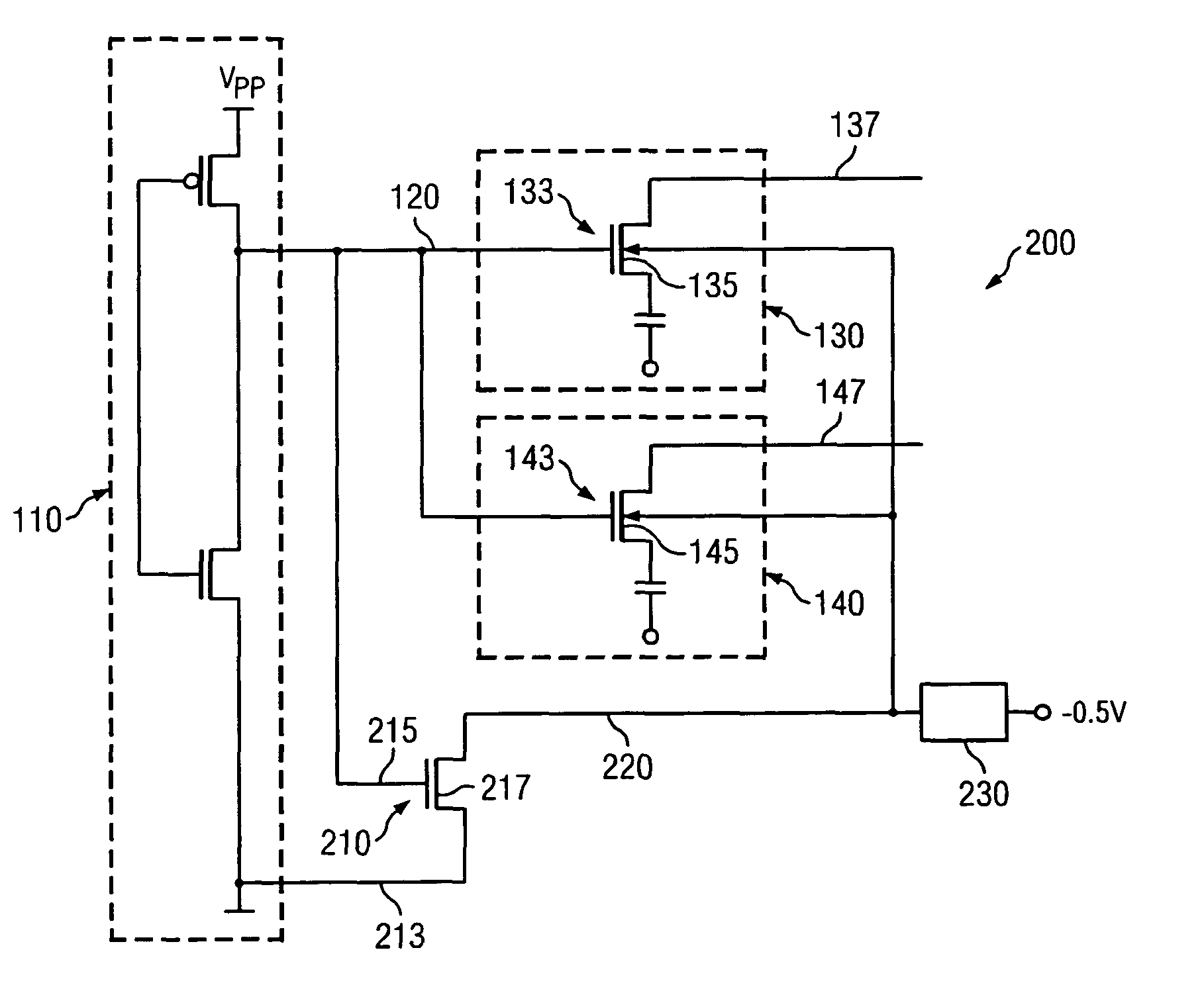
[0010]While the making and using of various embodiments of the present invention are discussed herein in terms of specific sensing schemes and voltage conditions, it should be appreciated that the present invention provides many inventive concepts that can be embodied in a wide variety of contexts. The specific embodiments discussed herein are merely illustrative of specific ways to make and use the invention, and are not meant to limit the scope of the invention.

[0011]The present invention provides a solution that can reduce the increase in the threshold voltage of dynamic random access memory (“DRAM”) devices, thereby improving device performance during operation. The use of body contacts as described herein can provide variable substrate voltages during DRAM operation. The body contacts can change the body bias of activated memory cells, while maintaining the body bias of inactive memory cells. This can reduce the body effect (i.e., variation of the threshold voltage due to a var...


PUM


Abstract

Active control of body contacts in memory devices can provide variable substrate voltages during device operation. The body contacts can be used to adjust the body bias of switches in activated memory cells, while maintaining the body bias of switches in inactive memory cells. This can reduce the body effect (i.e., variation of the threshold voltage due to a variation of the substrate or bulk voltage) and can therefore provide improved array device performance (e.g., reduced data corruption) while the word line (“WL”) is activated.

Description

FIELD OF THE INVENTION[0001]The invention relates generally to semiconductor memory integrated circuits (“ICs”), such as dynamic random access memories (“DRAMs”), and, more particularly, to a controlled substrate voltage for such ICs.BACKGROUND OF THE INVENTION[0002]Dynamic random access memories (“DRAMs”) are the most commonly manufactured product of all semiconductor integrated circuits (“ICs”). DRAMs are data storage devices that store data as a charge on a storage capacitor. A DRAM typically includes an array of memory cells. Each memory cell includes a storage capacitor and a transistor for transferring charges to and from the storage capacitor. Each memory cell is addressed by a word line (“WL”) and accessed by a bit line (“BL”) pair. The WL controls the transistor such that the transistor couples the storage capacitor to and decouples the storage capacitor from the BL pair for writing data to and reading data from the memory cell. Multiple word lines correspond to multiple ro...

Claims


Application Information

Patent Timeline
Patent Type & Authority Patents(United States)
IPC IPC(8): G11C16/04G11C5/14G11C11/404G11C11/4074G11C11/408
CPCG11C5/146G11C11/408G11C11/4074G11C11/404
Inventor POECHMUELLER, PETER
Owner POLARIS INNOVATIONS LTD
Why Eureka
Try Eureka