Overlay mark for aligning different layers on a semiconductor wafer

a technology of overlay marks and semiconductor wafers, applied in the field of overlay marks, can solve the problems of not meeting the requirements of the client, erroneous measurement of specifications, and the alignment between the pattern of the pre-layer and the pattern of the photoresist layer will not meet the accuracy requirements, so as to save the area cost

Active Publication Date: 2007-02-20
MACRONIX INT CO LTD
View PDF5 Cites 55 Cited by
  • Summary
  • Abstract
  • Description
  • Claims
  • Application Information

AI Technical Summary

Benefits of technology

[0011]The objective of the present invention is to provide an overlay mark for aligning different layers on a semiconductor wafer to avoid deviation and save the area cost.
[0013]Compared with the prior art technology, the present invention possesses the following advantages since the marks of different layers for checking alignment accuracy are positioned on the same area of the semiconductor wafer:

Problems solved by technology

Lack of proper alignment typically results in erroneous measurement of specification and fails to meet the requirements of the client.
If the overlay error is larger than an acceptable deviation value, the alignment between the pattern of the pre-layer and that of the photoresist layer will not meet the accuracy requirements.
As the design rule shrinks and the fabrication of the integrated circuits tends to use multi-layer design, the area cost issue of the bar-in-bar patterns becomes seriously high.

Method used


Image

  • Overlay mark for aligning different layers on a semiconductor wafer
  • Overlay mark for aligning different layers on a semiconductor wafer
  • Overlay mark for aligning different layers on a semiconductor wafer

Examples


first embodiment

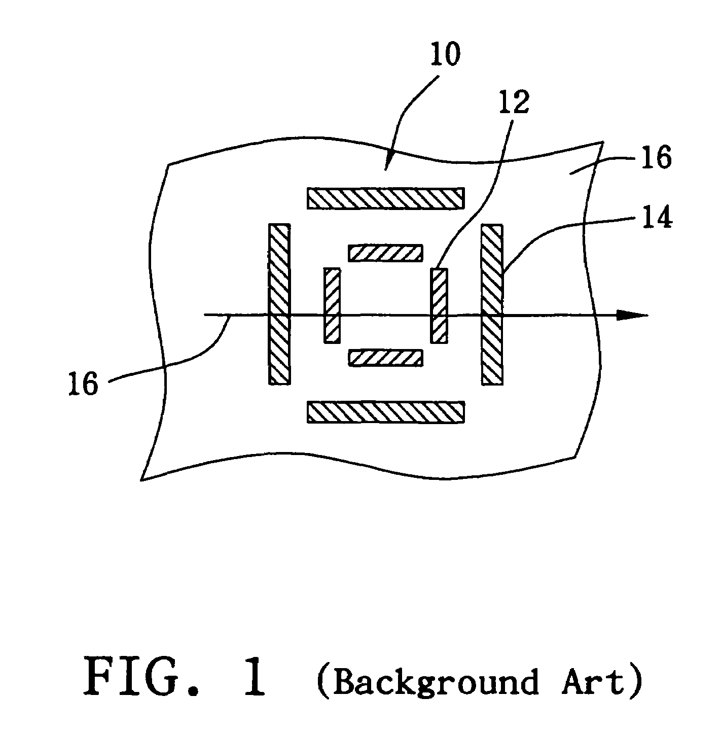
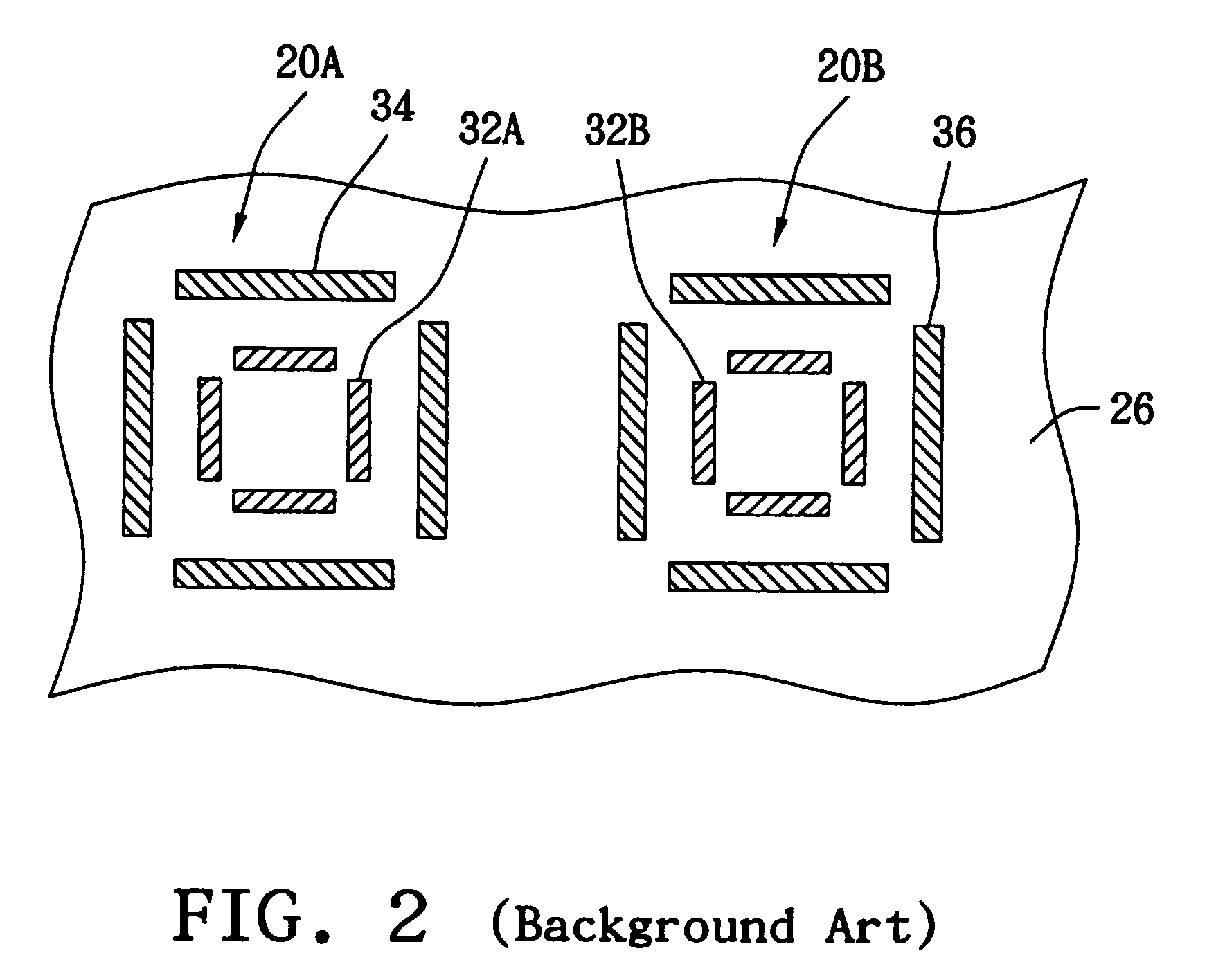
[0022]FIG. 3 is a top view of an overlay mark 100 for aligning different layers on a semiconductor wafer 102 according to the present invention. As shown in FIG. 3, the overlay mark 100 comprises a bar-in-bar mark 110 and two bar sets 120A, 120B on the semiconductor wafer 102. The bar-in-bar mark 110 comprises an inner bar mark 112 disposed on a first pre-layer and an outer bar mark 114 disposed on a second pre-layer. The inner bar mark 112 represents the pattern of a first pre-layer, and the outer bar mark 114 represents the pattern of a second pre-layer. The inner bar mark 112 comprises four bars, and the outer bar mark 114 comprises four bars outside the inner bar mark 112. The two bar sets 120A, 120B are perpendicular to each other, and each of two bar sets 120A, 120B comprises two parallel bars. The lengths of the two bar sets 120A, 120B are different, and the two bar sets 120A, 120B together form a rectangular pattern outside the bar-in-bar mark 110.

second embodiment

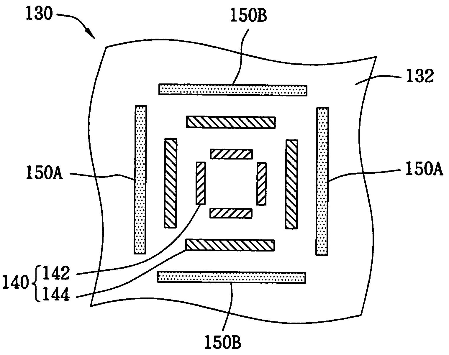
[0023]FIG. 4(a) to FIG. 4(d) are top views of an overlay mark 130 for aligning different layers on a semiconductor wafer 132 according to the present invention. As shown in FIG. 4(a), the lengths of the two bar set 150A, 150B are the same, and these two bar sets together form a square pattern outside a bar-in-bar mark 140 formed of an inner bar mark 142 and an outer bar mark 144. The two bar sets 150A, 150B can be positioned between the inner bar mark 142 and the outer bar mark 144, as shown in FIG. 4(b), or inside the bar-in-bar mark 140, as shown in FIG. 4(c). In addition, the bar-in-bar mark 140 and the two bar sets 150A, 150B can consist of segments patterns having a plurality of dot-marks, as shown in FIG. 4(d).

third embodiment

[0024]FIG. 5(a) and FIG. 5(b) are top views of an overlay mark 160 for aligning different layers on a semiconductor wafer 162 according to the present invention. As shown in FIG. 5(a), the overlay mark 160 comprises a first mark 170, a second mark 180 positioned outside the first mark 170 and a third mark 190 positioned outside the second mark 180. The first mark 170 represents the pattern of a first pre-layer, the second mark 180 represents the pattern of a second pre-layer, and the third mark 190 represents the pattern of a third layer on a semiconductor wafer 162. Compared with the overlay mark 130 shown in the FIG. 4(a), the first mark 170 can be regarded as being formed of four connected inner bars, and so can the second mark 180 and the third mark 190. Besides, the first mark 170, the second mark 180 and the third mark 190 can consist of segment patterns, as shown in FIG. 5(b).

[0025]Compared with the prior technology, the present invention possesses the following advantages si...


PUM

PropertyMeasurementUnit
lengthsaaaaaaaaaa
dimensionsaaaaaaaaaa
areasaaaaaaaaaa

Abstract

The present invention provides an overlay mark for aligning different layers on a semiconductor wafer. The overlay mark comprises a bar-in-bar mark and two bar sets on the semiconductor wafer. The bar-in-bar mark comprises an inner bar mark positioned in one of the pre-layer and an outer bar mark positioned in the other pre-layer. The two bar sets are perpendicular to each other, and each of two bar sets comprises two parallel bars. The bars can be connected and the lengths of the bars can be the same or different.

Description

BACKGROUND OF THE INVENTION[0001](A) Field of the Invention[0002]The present invention relates to an overlay mark for checking alignment accuracy, and more particularly, to an overlay mark for aligning different layers on a semiconductor wafer.[0003](B) Description of the Related Art[0004]Nowadays, the semiconductor devices and integrated circuits include multi-layer structures having dimensions smaller than one micrometer. Proper alignment of different layers is essential for proper performance of the fabricated semiconductor devices and circuits. Overlay measurements are routinely performed to verify the proper alignment. Lack of proper alignment typically results in erroneous measurement of specification and fails to meet the requirements of the client.[0005]Overlay measurements optically measure the relative positions of the overlay marks on different layers of a structure on the semiconductor wafer. More particularly, a rectangular overlay mark is formed on each layer of the st...

Claims


Application Information

Patent Timeline
Patent Type & Authority Patents(United States)
IPC IPC(8): G01B11/00H01L23/544G01B11/27G03F7/20
CPCG03F7/70633G01B11/272
Inventor LIN, YEN YU
Owner MACRONIX INT CO LTD
Why Eureka
Try Eureka