Stacked packages and systems incorporating the same

a technology of stacking packages and stacking components, applied in the field of microelectronic packaging and systems, to achieve the effect of facilitating signal routing and minimizing the complexity of signal routing

Active Publication Date: 2007-02-27
TESSERA INC
View PDF29 Cites 86 Cited by
  • Summary
  • Abstract
  • Description
  • Claims
  • Application Information

AI Technical Summary

Benefits of technology

[0005]One aspect of the present invention provides a stacked packaging arrangement especially useful for, e.g., logic chips such as field programmable gate arrays (hereinafter “FPGA”) or microprocessors, in which the stacked packaging arrangement accommodates logical interconnections between chips where inputs from one chip are connected to outputs of other chips. A further aspect of the invention provides designs for individual units and elements which can be used in such stacked arrangement. Yet another aspect of the invention provides a system-level design which allows for integration of multiple stacked packages while minimizing the complexity of signal routing in a printed circuit board (“PCB”) or other circuit panel used in the system. Still other aspects of the invention provide unit configurations which facilitate routing of signals to chips on different packages in a stack.

Problems solved by technology

Even in these situations, it is sometimes necessary to provide different packages for different chips in the stack.

Method used


Image

  • Stacked packages and systems incorporating the same
  • Stacked packages and systems incorporating the same
  • Stacked packages and systems incorporating the same

Examples


Embodiment Construction

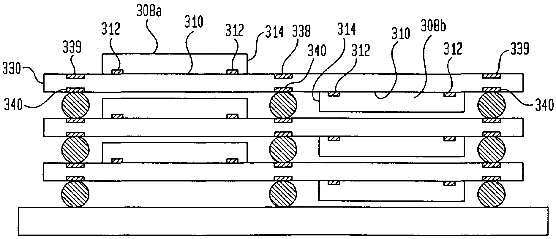
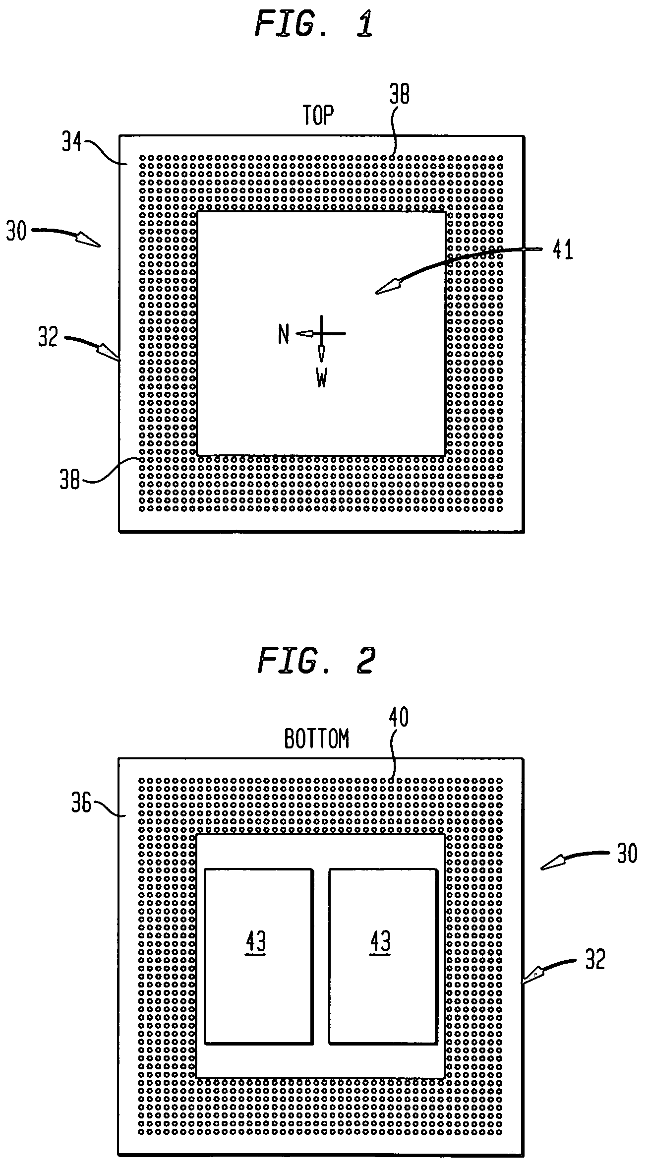
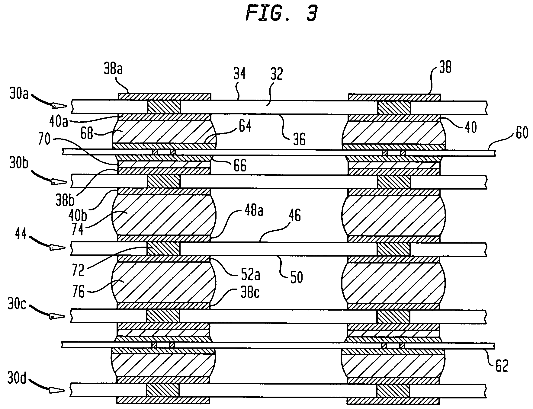
[0024]A system according to one embodiment of the invention uses a plurality of units 30 (FIGS. 1 and 2). Each unit includes a unit substrate 32 in the form of a dielectric element such as a circuit board or flexible circuit panel, commonly referred to as a “tape.” The unit substrate defines a top side 34 (FIG. 1) and a bottom side 36 (FIG. 2). Each unit substrate has top unit terminals 38 exposed at the top side of the unit and bottom unit terminals 40 exposed at its bottom side.

[0025]Each unit also includes a first microelectronic element in the form of a semiconductor chip 41, in this case, an FPGA. In the particular design illustrated, each unit also includes additional semiconductor chips or SRAMs 43. The SRAM within each unit cooperates with the FPGA of that particular unit. In the embodiment illustrated, the FPGA chip is flip-chip mounted to the top of the unit substrate, so that the unit substrate serves as the package for the FPGA. The SRAMs are supplied in separate chip si...


PUM


Abstract

A microelectronic assembly incorporates units stacked one above the other and may include a plurality of similar stacks mounted to a circuit board. Some of the stacks may be inverted, rotated or both relative to other stacks so that corresponding edges of the stacks face one another to facilitate communication between the stacks. Communication between the stacks may be carried along traces on one or more interposers intercepting the stacks remote from the circuit board. Within each stack, conducting paths may extend in vertical columns or in other arrangements such as a stair step arrangement wherein each conductive path traverses a series of column positions, or in a crossing arrangement such two conductive paths cross back and forth between column positions along the vertical extend of the stack. A stack may include portions disposed above and below the circuit board.

Description

CROSS-REFERENCE TO RELATED APPLICATIONS[0001]This application claims the benefit of the filing date of U.S. Provisional Patent Application No. 60 / 517,179, filed Nov. 4, 2003, the disclosure of which is hereby incorporated by reference herein.FIELD OF THE INVENTION[0002]The present invention relates to microelectronic packaging and systems.BACKGROUND OF THE INVENTION[0003]Microelectronic elements such as semiconductor chips are commonly provided in packages having terminals connected to the microelectronic element itself, such terminals being available for connection to external elements such as printed circuit boards.[0004]Some microelectronic elements, notably memory chips, have been provided heretofore in stacked arrangements with packages superposed one atop the other to conserve space on a circuit board. Such structures typically involve only a few chips and relatively simple connections which normally do not involve interconnections between chips in the stack, or between multip...

Claims


Application Information

Patent Timeline
Patent Type & Authority Patents(United States)
IPC IPC(8): H01L23/34H01L23/02
CPCH01L25/10H05K1/112H01L24/17H01L25/105H01L2225/0652H01L2225/06548H01L2225/06572H05K1/141H05K3/3436H05K2201/10378H05K2201/10515H01L2225/06527H01L2224/16225H01L2225/1023H01L2225/107H01L2924/15311H01L2924/1437H01L25/0655H01L2224/48091H01L2924/00014H01L23/49816H01L23/49833H01L23/4985H01L24/14
Inventor GIBSON, DAVIDSTAVROS, ANDY
Owner TESSERA INC
Why Eureka
Try Eureka