Single-poly EEPROM

a single-poly, eeprom technology, applied in the direction of solid-state devices, semiconductor devices, instruments, etc., can solve the problems of increased cost, increased process steps, and several drawbacks of the prior art cell b>10/b>, and achieves increased erasure efficiency, wide process window, and increased voltage difference

Active Publication Date: 2007-03-20
UNITED MICROELECTRONICS CORP
View PDF3 Cites 5 Cited by
  • Summary
  • Abstract
  • Description
  • Claims
  • Application Information

AI Technical Summary

Benefits of technology

[0007]It is therefore a primary objective of the present invention to provide a single-poly EPPROM, which has high erase efficiency and can be fabricated with conventional CMOS process sequences.
[0010]The present invention utilizes the avalanche breakdown generated in a junction region of the P-well and the N+ doped region underneath the floating gate. Thereby, hot holes inject into a floating gate to neutralize the trapped electrons and Fowler-Nordheim tunneling is utilized to pull out electrons from the floating gate for executing erasure. Therefore, a single-poly EPPROM of the present invention has the following advantages:
[0011]1. The present invention utilizes a low voltage to execute an erasure operation so that the single-poly EPPROM can be fabricated with conventional CMOS process sequences without any extra process step for saving production costs.
[0012]2. The present invention utilizes the avalanche hot hole injection mechanism, whose operation speed is faster than Fowler-Nordheim tunneling, and the program / erasure cycle and the testing costs are reduced.
[0014]4. The present invention further includes a P+ doped guard ring underneath the floating gate in the P-well for increasing the erasure efficiency and increasing the voltage difference between the floating gate and the P+ doped guard ring to give a wide process window.

Problems solved by technology

However, the above-described EEPROM cell 10 of the prior art suffers from several drawbacks.
Second, the EEPROM cell 10 needs an extra channel stop region 38 and formation of conductor 36 for connecting two gates, this, in turns, means extra process steps and thus raised cost.

Method used


Image

  • Single-poly EEPROM
  • Single-poly EEPROM
  • Single-poly EEPROM

Examples


Embodiment Construction

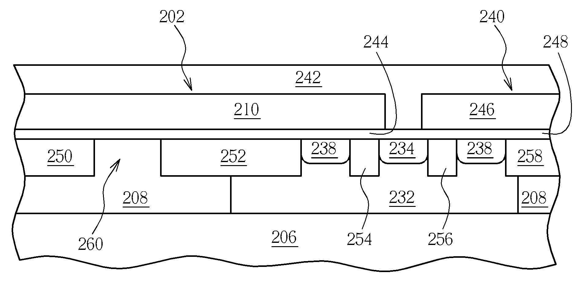
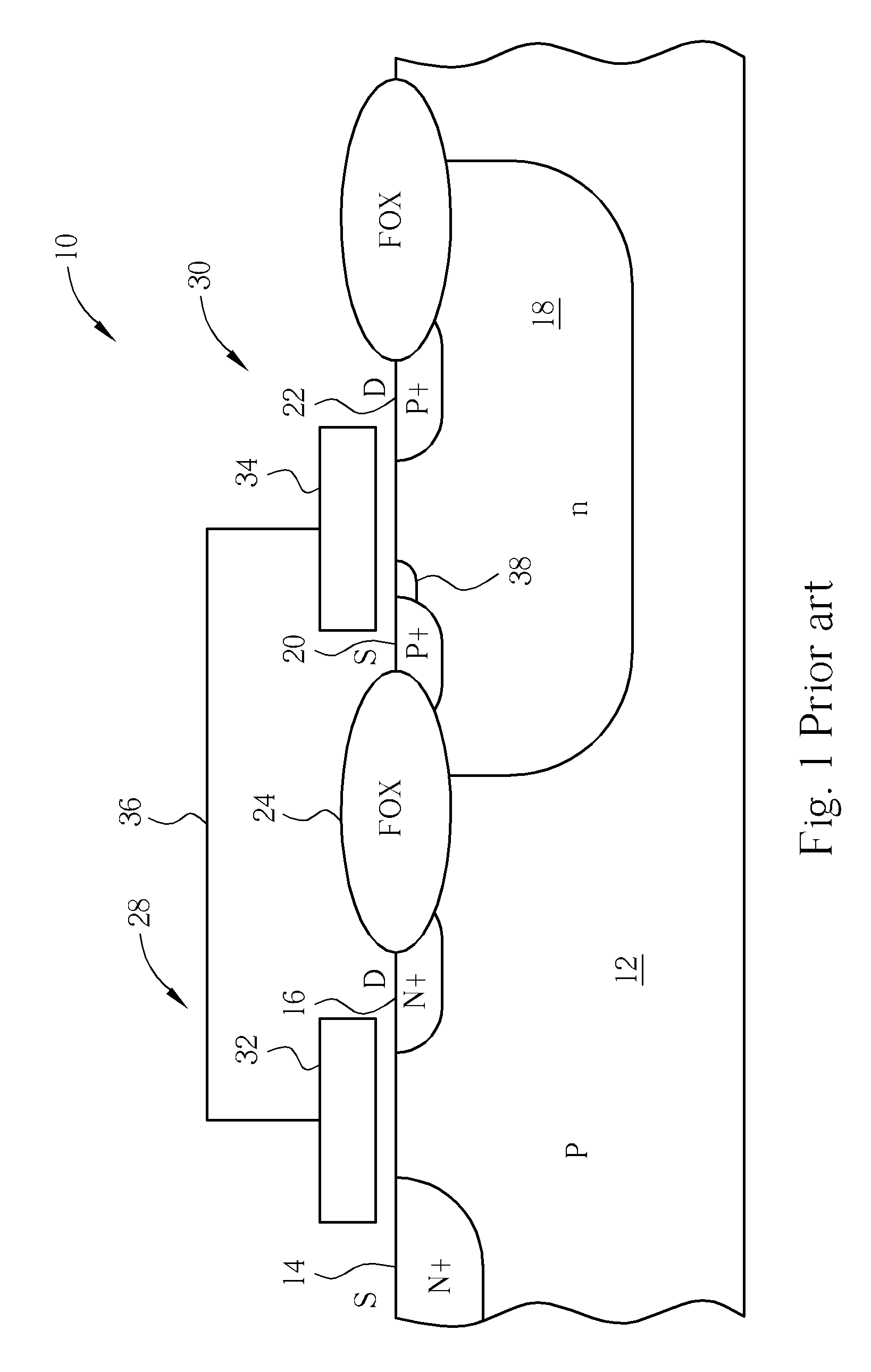
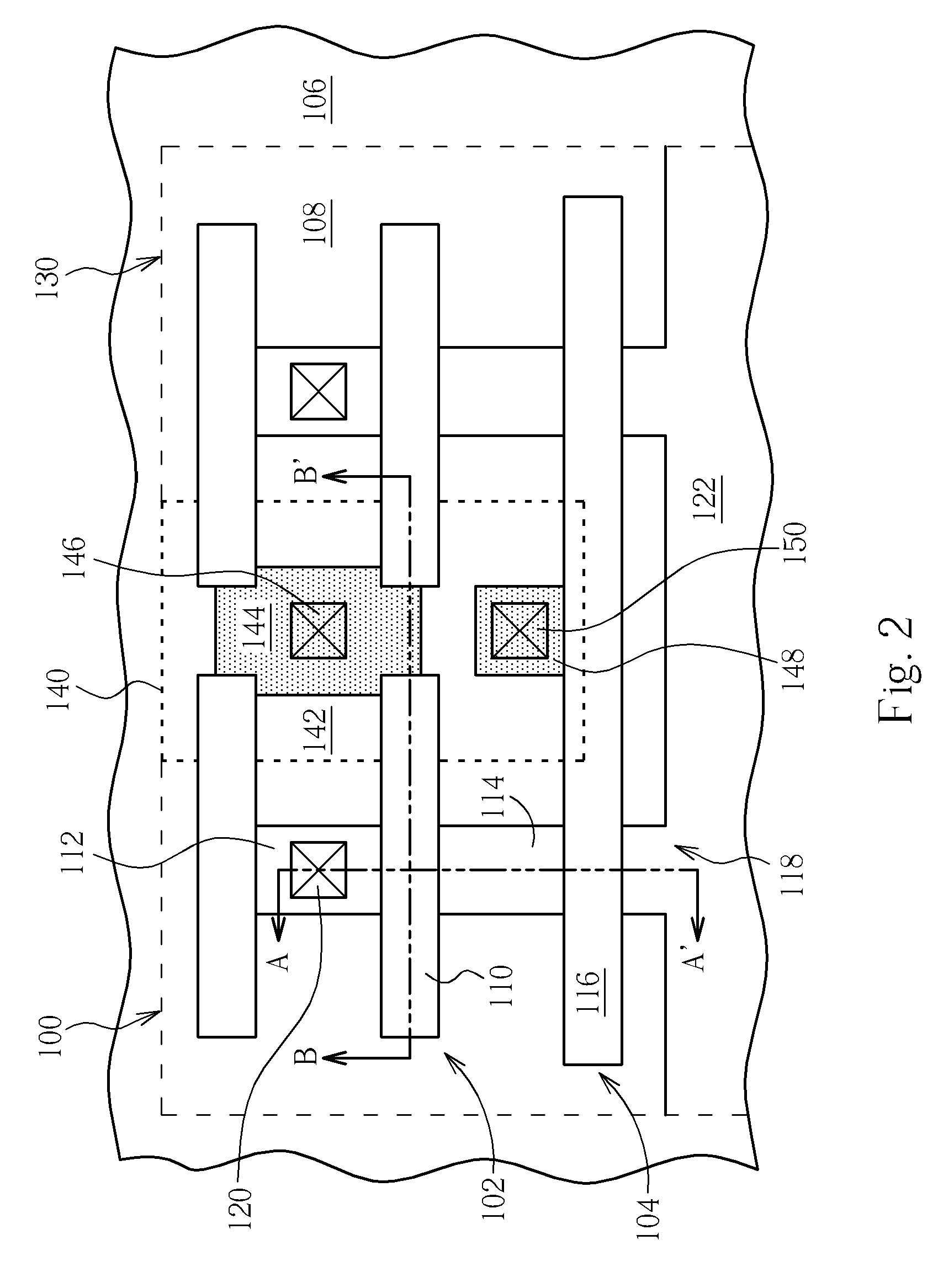
[0024]Please refer to FIG. 2. FIG. 2 is a plane view schematically illustrating a partial layout of a single-poly EEPROM according to a first preferred embodiment of the present invention. As shown in FIG. 2, a single-poly EEPROM unit 100 includes a first PMOS transistor 102 and a second PMOS transistor 104 serially connected to the first PMOS transistor 102. The first PMOS transistor 102 and the second PMOS transistor 104 are formed on an N-well 108, as indicated by the dashed line in FIG. 2, of a P type substrate 106. The first PMOS transistor 102 includes a floating gate 110, a first P+ doped drain region 112, and a first P+ doped source region 114. The second PMOS transistor 104 includes a gate 116 and a second P+ doped source region 118, and the first P+ doped source region 114 of the first PMOS transistor 102 serves as a drain of the second PMOS transistor 104, thereby electrically connecting the first PMOS transistor 102 with the second PMOS transistor 104.

[0025]It is underst...


PUM


Abstract

The single-poly EEPROM includes a first PMOS transistor serially connected to a second PMOS transistor. The first and second PMOS transistors are both formed on an N-well of a P type substrate. The first PMOS transistor includes a floating gate, a first P+ doped drain region and a first P+ doped source region. The second PMOS transistor includes a gate and a second P+ doped source region. The first P+ doped drain region of the first PMOS transistor serves as a drain of the second PMOS transistor. A diode is located in the P type substrate including a P-well and a N+ doped region. The floating gate overlaps with the N-well and extends to the N+ doped region. The overlapped region of the P-well and the N+ doped region junction beneath the floating gate serves as an avalanche injection point in the vicinity of the first PMOS transistor.

Description

BACKGROUND OF INVENTION[0001]1. Field of the Invention[0002]The present invention relates to a single-poly electrically erasable programmable read only memory (EEPROM), and more particularly, to a single-poly EEPROM, which has high erasure efficiency.[0003]2. Description of the Prior Art[0004]Electronic memory comes in a variety of forms to serve a variety of purposes. Flash electrically erasable programmable read only memory (flash EEPROM) is used for easy and fast information storage in such devices as personal digital assistants (PDA), digital cameras and home video game consoles. Generally, an EEPROM chip has a grid of columns and rows with a cell that has two transistors at each intersection. One of the transistors is known as a floating gate, and the other one is the control gate. The floating gate's only link to the row, or word line, is through the control gate. As long as this link is in place, the cell has a value of 1. Changing the value to a 0 requires a well-known proce...

Claims


Application Information

Patent Timeline
Patent Type & Authority Patents(United States)
IPC IPC(8): H01L29/788
CPCG11C16/0416H01L29/7883H01L27/11521H01L27/11558H01L27/115G11C2216/10H10B41/60H10B69/00H10B41/30
Inventor PENG, NAI-CHENHUANG, SHUI-CHINLEE, TZYH-CHEANGWANG, CHUAN FULIN, SUNG-BIN
Owner UNITED MICROELECTRONICS CORP
Why Eureka
Try Eureka