Semiconductor memory device and operating method thereof

a semiconductor memory and operating method technology, applied in the field of semiconductor memory devices, can solve the problems of comparatively lower read and write speeds of nonvolatile memory devices than those of volatile memory devices, and achieve the effect of improving the erase efficiency of semiconductor memory devices

Active Publication Date: 2018-05-31
SK HYNIX INC
View PDF1 Cites 6 Cited by
  • Summary
  • Abstract
  • Description
  • Claims
  • Application Information

AI Technical Summary

Benefits of technology

[0008]Various embodiments are directed to a semiconductor memory device capable of improving erase efficiency of the semiconductor memory device and an operating method thereof.

Problems solved by technology

However, read and write speeds of a nonvolatile memory device are comparatively lower than those of a volatile memory device.

Method used


Image

  • Semiconductor memory device and operating method thereof
  • Semiconductor memory device and operating method thereof
  • Semiconductor memory device and operating method thereof

Examples


Embodiment Construction

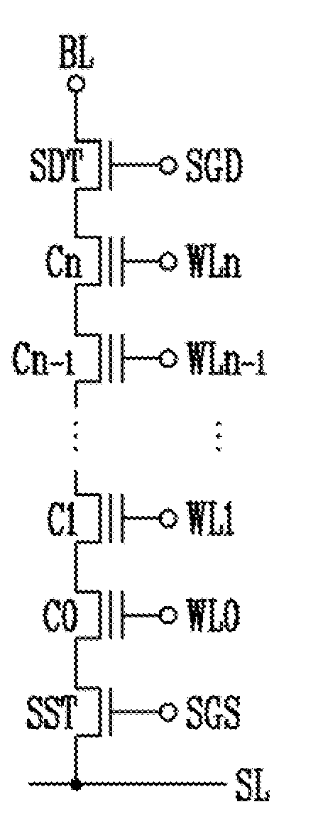
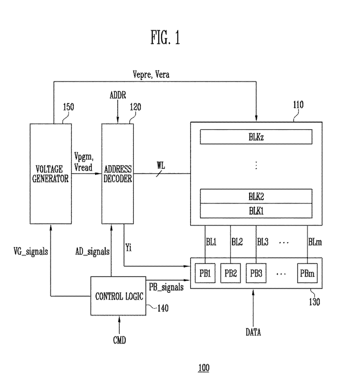
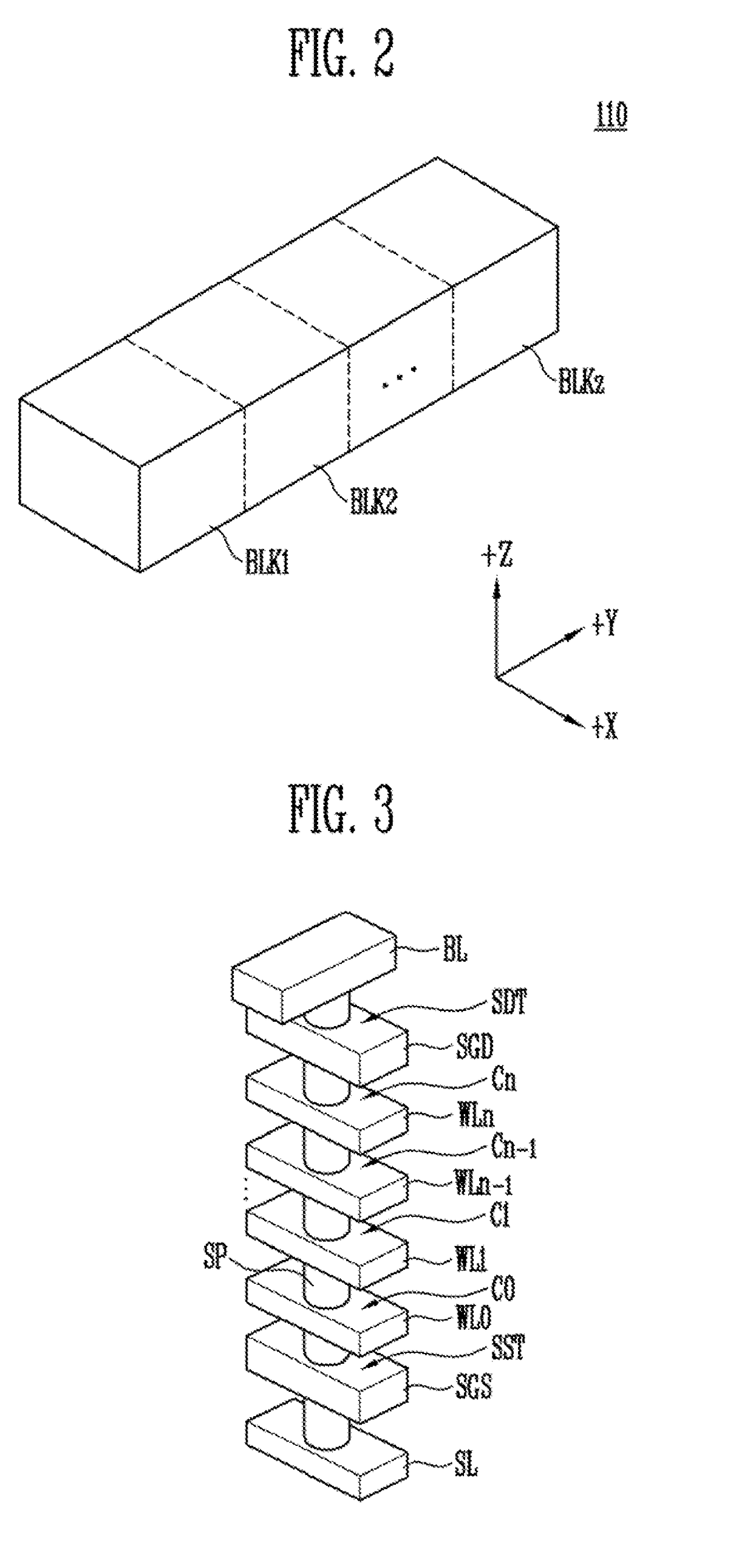
[0026]Hereinafter, embodiments of the present invention will be described in greater detail with reference to the accompanying drawings. However, we note that the present invention may be embodied in different forms and should not be construed as being limited to the embodiments set forth herein. Rather these embodiments are provided so that this disclosure will be thorough and complete, and will fully convey the scope of the described embodiments to those skilled in the art to which the present invention pertains.

[0027]In the drawings, dimensions may be exaggerated for clarity of illustration. It will be understood that when an element is referred to as being “between” two elements, it can be the only element between the two elements, or one or more intervening elements may also be present. Like reference numerals refer to like elements throughout.

[0028]Also, the drawings are simplified schematic illustrations of the various embodiments and their various features. As such, well-kno...


PUM


Abstract

A semiconductor memory device includes a memory cell array including a plurality of memory blocks, a voltage generator suitable for applying an erase voltage to a source line of at least one memory block selected from among the plurality of memory blocks during an erase operation, a read and write circuit suitable for applying an initial setting voltage, to bit lines of at least one memory block during the erase operation, and a control logic suitable for controlling the voltage generator and the read and write circuit to apply the initial setting voltage to the bit lines before applying the erase voltage to the source line.

Description

CROSS-REFERENCE TO RELATED APPLICATION[0001]The present application claims priority under 35 U.S.C. § 119(a) to Korean patent application number 10-2016-0158939, filed on Nov. 28, 2016, the entire disclosure of which is incorporated herein by reference in its entirety.BACKGROUNDField of Invention[0002]Various embodiments of the invention relate generally to an electronic device, and more particularly, to a semiconductor memory device and an operating method thereof.Description of Related Art[0003]Semiconductor memory devices are generally classified into volatile and nonvolatile memory devices.[0004]Unlike a volatile memory device, a nonvolatile memory device can, maintain data stored therein even when a power supply to the device is interrupted. However, read and write speeds of a nonvolatile memory device are comparatively lower than those of a volatile memory device. Therefore, nonvolatile memory devices may be employed in applications requiring maintaining the stored data regard...

Claims


Application Information

Patent Timeline
Patent Type & Authority Applications(United States)
IPC IPC(8): G11C16/14G11C16/10G11C16/26G11C16/04
CPCG11C16/14G11C16/0483G11C16/26G11C16/10G11C16/24G11C16/30G11C16/08G11C16/16G11C16/32
Inventor PARK, EUN YOUNG
Owner SK HYNIX INC
Why Eureka
Try Eureka