Delivery regions for power, ground and I/O signal paths in an IC package

a technology applied in the field of integrated circuit packages, can solve the problems of high inductance and resistance of power and ground paths, electromagnetic interference in delivering error-free signaling, and difficulty in delivering stable power to the chip

Inactive Publication Date: 2007-04-24
INTEL CORP
View PDF9 Cites 43 Cited by
  • Summary
  • Abstract
  • Description
  • Claims
  • Application Information

AI Technical Summary

Problems solved by technology

The higher power requirements require more power and ground paths that take up more area in the chip carrier and socket, causing difficulties in delivering stable power to the chip.
One difficulty with these high performance chips is the close proximity of the power paths and I / O signal paths in the IC packages and sockets, which may result in electromagnetic interference in delivering error free signaling.
Another difficulty is the high inductance and resistance of the power and ground paths.
For example, a fast increase in the current drawn by the processor chip may cause a drop in the power supply voltage, since the high rate of change in current is through the inductance of the chip carrier and the socket.

Method used


Image

  • Delivery regions for power, ground and I/O signal paths in an IC package
  • Delivery regions for power, ground and I/O signal paths in an IC package
  • Delivery regions for power, ground and I/O signal paths in an IC package

Examples


Embodiment Construction

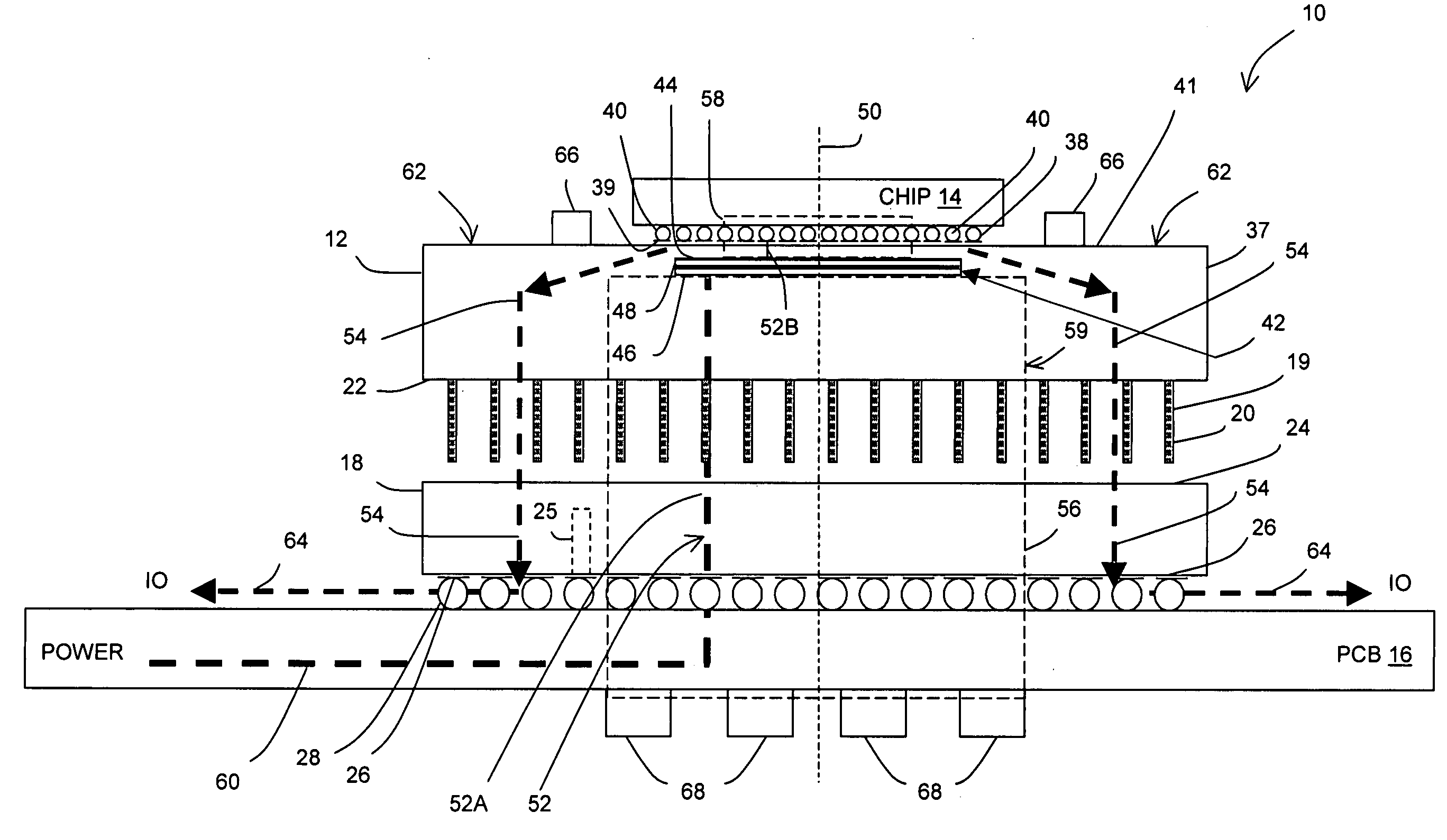
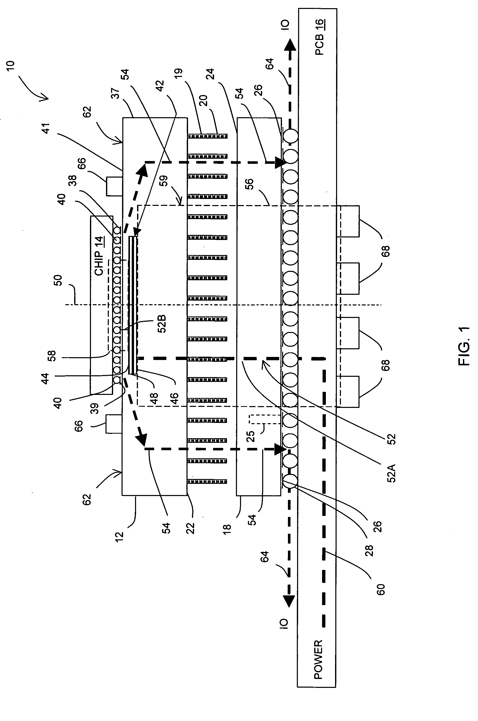
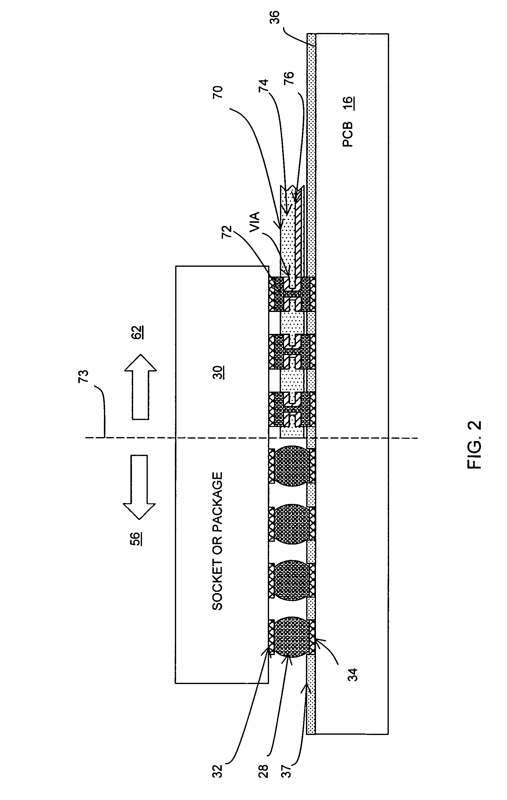
[0012]In the following description, for purposes of explanation, numerous details are set forth in order to provide a thorough understanding of the disclosed embodiments of the present invention. However, it will be apparent to one skilled in the art that these specific details are not required in order to practice the disclosed embodiments of the present invention. In other instances, well-known electrical structures and circuits are shown in block diagram form in order not to obscure the disclosed embodiments of the present invention.

[0013]Referring to FIG. 1, there is shown an electronic assembly 10 in accordance to one embodiment of the present invention. The electronic assembly 10 may include an integrated circuit (IC) package 12 having mounted therein a silicon chip or die 14 containing an IC, a substrate or printed circuit board (PCB) 16, and a socket 18 mounted between the IC package 12 and the PCB 16 (package 12 is shown detached from socket 18 in FIG. 1). Although the sock...


PUM


Abstract

An integrated circuit (IC) package includes a chip carrier and a chip mounted to the chip carrier. The chip carrier has a centrally located power delivery region and a peripherally located input-output (I / O) delivery region disposed in partially surrounding relationship to the power delivery region. Power and ground paths are disposed in the power delivery region and I / O signal paths are disposed in the I / O delivery region.

Description

BACKGROUND OF THE INVENTION[0001]1. Field of the Invention[0002]The present invention relates to electronic devices, and in particular, to integrated circuit packages.[0003]2. Description of Related Art[0004]An integrated circuit (IC) package includes a chip carrier and a silicon die or chip mounted in the chip carrier, such chip including an integrated circuit. The IC package provides the means to bring input / output (I / O) signals and a voltage supply in and out of the chip. Generally, there are two interconnection levels of the IC package: the chip to the chip carrier and the chip carrier to a substrate or printed circuit board (PCB). The IC package may be directly coupled to the PCB or indirectly coupled to the PCB through a socket so that the IC package is removable.[0005]As semiconductor chips and other devices are required to perform more functions or operations in shorter periods of time, power and signal requirements for chips are increasing. High speed performance chips, ope...

Claims


Application Information

Patent Timeline
Patent Type & Authority Patents(United States)
IPC IPC(8): H05K1/11H01L23/50H05K1/14H05K7/06H05K7/10
CPCH01L23/50H05K1/112H05K1/147H05K7/1092H01L2224/16H01L2924/15312H01L2924/19105H01L2924/3011H05K1/141H05K2201/09227H05K2201/094H05K2201/10325H05K2201/10689H05K2201/10734H01L2924/01019H01L2924/10253H01L2924/00
Inventor PROKOFIEV, VICTORPALANDUZ, CENGIZ A.
Owner INTEL CORP
Why Eureka
Try Eureka