Method for conditioning a microelectronics device deposition chamber

a technology of microelectronics and deposition chambers, which is applied in the direction of coatings, semiconductor devices, chemical vapor deposition coatings, etc., can solve the problems of increased metal density, defects in the device at subsequent deposition, and contamination still occurring in the deposition chamber despite, and achieves high gas flow

Active Publication Date: 2007-07-10
TEXAS INSTR INC
View PDF5 Cites 14 Cited by
  • Summary
  • Abstract
  • Description
  • Claims
  • Application Information

AI Technical Summary

Problems solved by technology

While every step is taken to reduce or eliminate the possibility of contaminate particles, contamination still occurs within the deposition chamber despite the best of efforts.
Until recently, this has seemed to be an adequate practice, but as devices sizes have continued to shrink deep into the sub-micron range, it has been noticed that defects are occurring in the devices at subsequent deposition steps, even though acceptable particle defectivity measurements are being obtained.
It is believed that one reason for this is that as device sizes shrink, the metal density increases and any particle has a greater chance of causing a failure on the wafer.
Thus, it is apparent that present pre-conditioning processes are not adequate to assure minimization of wafer to wafer particle defects.

Method used


Image

  • Method for conditioning a microelectronics device deposition chamber
  • Method for conditioning a microelectronics device deposition chamber
  • Method for conditioning a microelectronics device deposition chamber

Examples


Embodiment Construction

[0018]The present invention recognizes the heretofore unknown problem of residual liquefied gas residing in a supply line connected to a deposition chamber and the substantial particle reduction benefits associated with removing that residual liquefied gas prior to depositing a layer onto a microelectronics wafer.

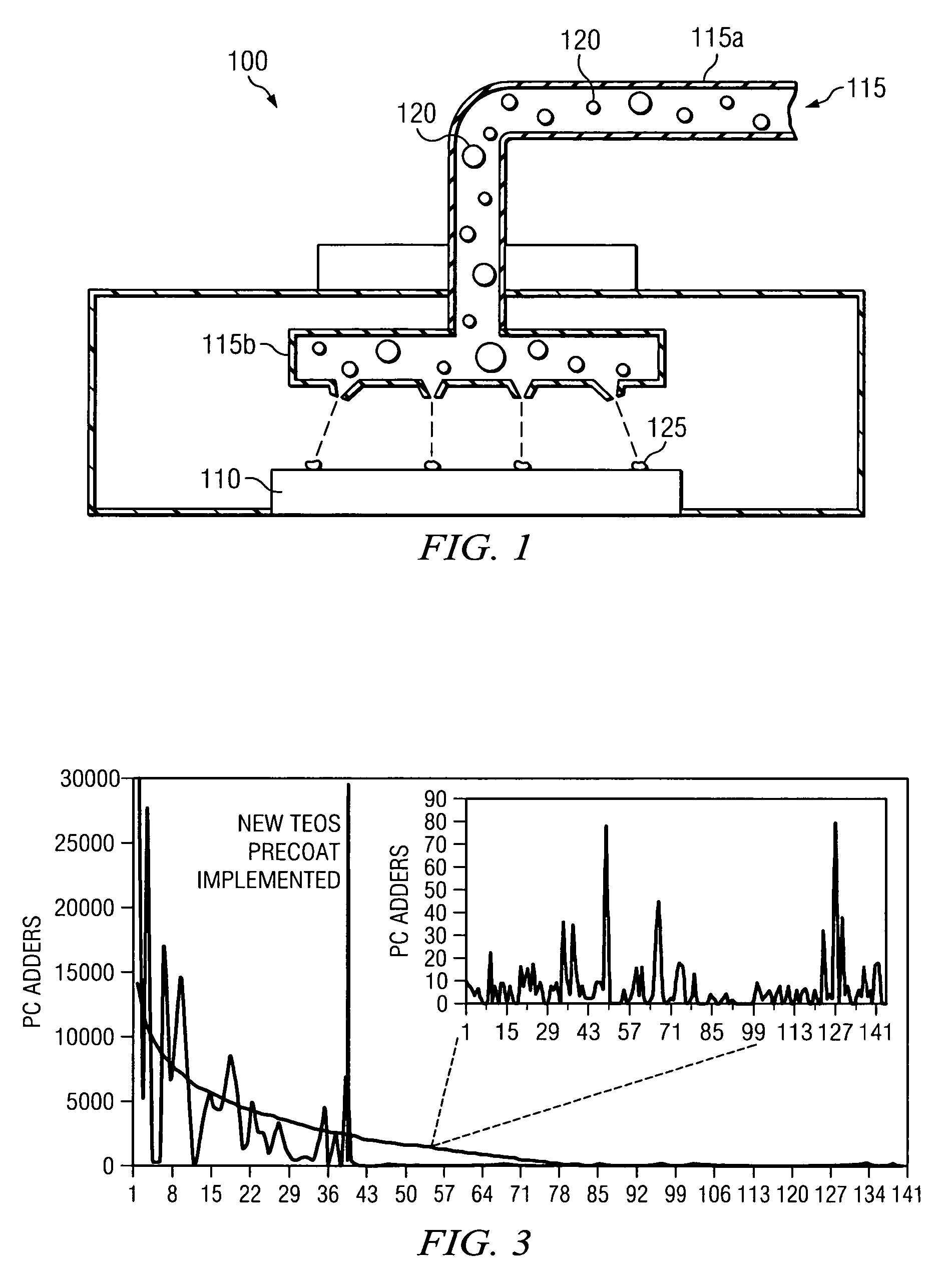
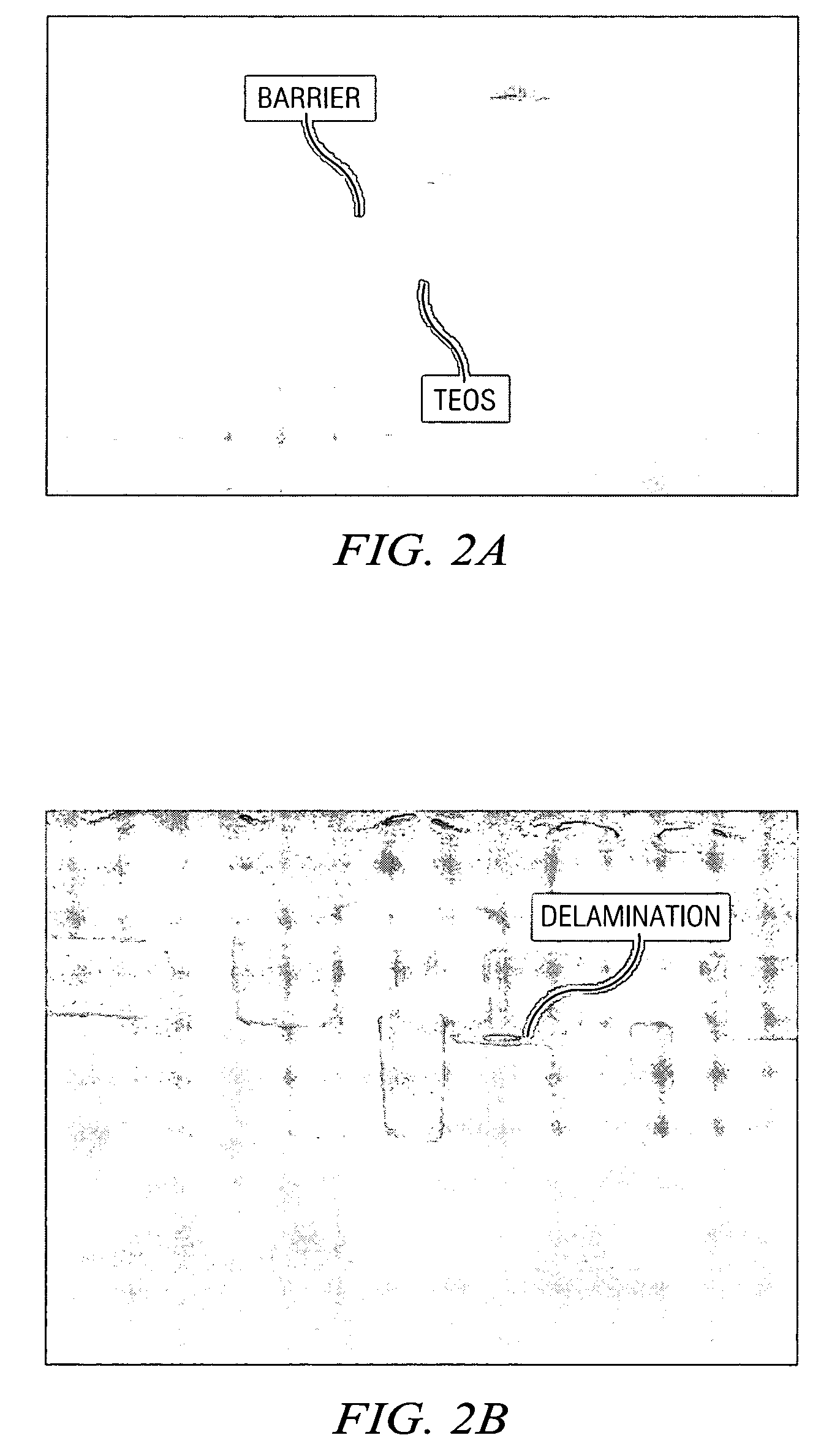
[0019]Referring initially to FIG. 1, there is illustrated a schematic drawing of a deposition chamber 100 having a microelectronics wafer 110 located therein and a supply line 115 that is connected to and includes a line 115a and shower head 115b through which gas is dispensed in the deposition chamber 100 to form a deposition plasma. It should be understood that this figure is a simplified, highly schematic view of a deposition chamber that can be found in a conventional deposition tool and that the configuration of the deposition tool and chamber will vary from one manufacturer to another. Moreover, the scope of the present invention is not limited to any one type of depo...


PUM

PropertyMeasurementUnit
pressureaaaaaaaaaa
pressureaaaaaaaaaa
poweraaaaaaaaaa

Abstract

The present invention provides, in one aspect, a method of conditioning a deposition chamber 100. An undercoat is placed on the walls of a deposition chamber 100 and a pre-deposition coat is deposited over the undercoat with a plasma gas mixture conducted at a high pressure and with high gas flow.

Description

TECHNICAL FIELD OF THE INVENTION[0001]The present invention is directed in general to a pre-deposition conditioning method for a microelectronics device deposition chamber, and more specifically, to a method of removing residual liquefied gas within a supply line of a deposition tool that is used to fabricate a microelectronics device.BACKGROUND[0002]Microelectronic circuits have shrunk well into the sub-micron range, and their size continues to shrink even smaller with each passing generation of technology. As this miniaturization continues, each step of the manufacturing process becomes even more critical to assure as great a yield of defect-free devices as possible. Even the most initial and seemingly insignificant steps of the manufacturing process are important in assuring commercially feasible device yields.[0003]One area that has grown in importance as device sizes have shrunk is the deposition chamber that is used to deposit the various layers that make up a microelectronics...

Claims


Application Information

Patent Timeline
Patent Type & Authority Patents(United States)
IPC IPC(8): H01L21/44
CPCC23C16/4404H01L21/31612H01L21/768Y10S438/903H01L21/02164
Inventor PAVONE, SALVATOR F.NEW, JASON J.
Owner TEXAS INSTR INC
Why Eureka
Try Eureka