Semiconductor light-emitting apparatus having wavelength conversion portion and method of fabricating the same

a technology of semiconductors and light-emitting devices, which is applied in the direction of chemistry apparatus and processes, lasers, and light-emitting compositions. it can solve the problems of increased white chip costs, uneven color, and difficulty in manufacturing, and achieves low cost, low profile, and great ease.

Active Publication Date: 2007-08-21
STANLEY ELECTRIC CO LTD
View PDF14 Cites 32 Cited by
  • Summary
  • Abstract
  • Description
  • Claims
  • Application Information

AI Technical Summary

Benefits of technology

[0025]As described above, other aspects of the invention provide suitable methods for fabricating the semiconductor light-emitting apparatus that have wavelength conversion layers. In accordance with these particular aspects of the invention, it is possible to fabricate a semiconductor light-emitting apparatus of low profile with great ease and / or at low cost.
[0026]In accordance with another aspect of the invention, it is possible to obtain light emission with significantly high efficiency as compared to apparatuses that utilize only the light transmitted through a wavelength conversion layer or only the light reflected from a wavelength conversion layer. Moreover, since the process of forming a curved area in the concave portion may not be required, a low-profile apparatus can be fabricated at low cost. In addition, light-emitting apparatuses of this type can be manufactured by using conventional LED lead frames as is, which can eliminate the need for special molds.
[0027]In accordance with another aspect, the excitation light that is emitted in every direction from the semiconductor light-emitting device can generally undergo sufficient wavelength conversion before being emitted out of the light-emitting apparatus. This means a significant improvement to reducing color unevenness and intensity unevenness. In particular, when near-ultraviolet light is used as the excitation light source, the configuration capable of reducing intensity unevenness and suppressing the transmission of the near-ultraviolet light can prevent a light guide plate and the like from ultraviolet degradation. Moreover, when constituent light sources of white light, such as blue light, are used as the excitation light source, it is possible to fabricate a white LED of reduced color unevenness and intensity unevenness.

Problems solved by technology

As a result, there have been problems relating to increased costs for the white chip LED, difficulty in manufacturing, etc.
In terms of intensity (intensity distribution), there have been problems in that the intensity peaks at the area immediately near the semiconductor light-emitting device 12 and it decreases toward the periphery.
That is, unevenness in color has also occurred in this case.
As for intensity distribution, there have also been problems similar to the intensity problems described above.

Method used


Image

  • Semiconductor light-emitting apparatus having wavelength conversion portion and method of fabricating the same
  • Semiconductor light-emitting apparatus having wavelength conversion portion and method of fabricating the same
  • Semiconductor light-emitting apparatus having wavelength conversion portion and method of fabricating the same

Examples


Embodiment Construction

[0037]Hereinafter, description will be given of the present invention with reference to the drawing figures, wherein like reference numerals designate identical or corresponding elements throughout the several figures. Incidentally, various modifications can be made without departing from the gist of the invention. It is intended that various modifications of the exemplary embodiments described herein can be made and would fall within the scope of the present invention.

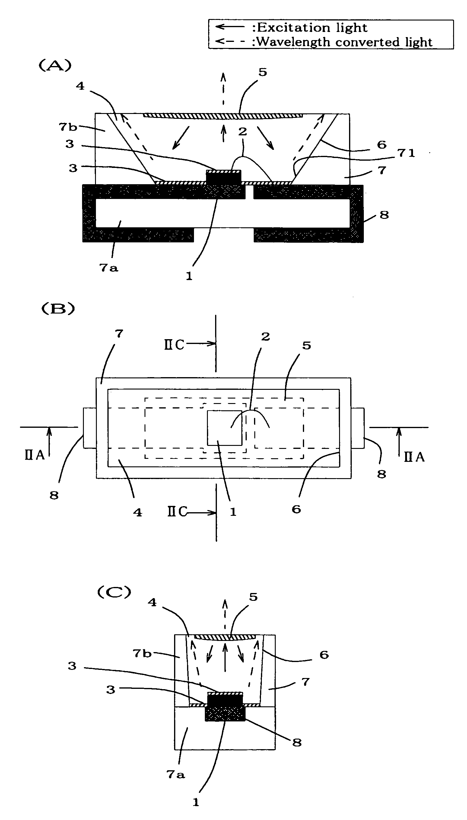
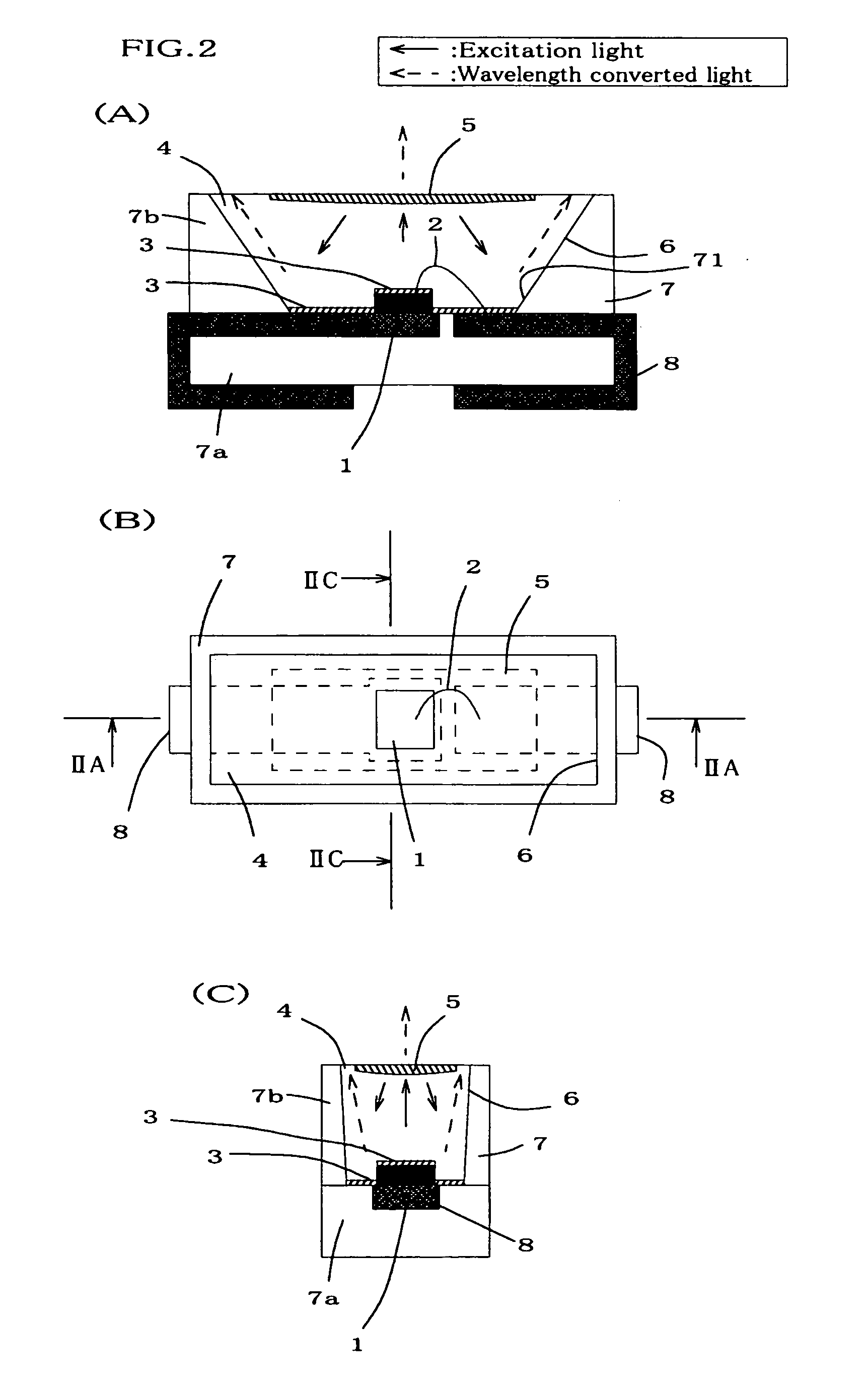
[0038]FIGS. 2A-2C are explanatory diagrams showing an embodiment of the semiconductor light-emitting apparatus made in accordance with the principles of the invention. FIG. 2A is a sectional view taken along the line IIA-IIA of FIG. 2B. FIG. 2B is a schematic plan view. FIG. 2C is a sectional view taken along the line IIC-IIC of FIG. 2B.

[0039]The semiconductor light-emitting apparatus of FIG. 2A can include an insulating base 7, a semiconductor light-emitting device 1, and a wavelength conversion portion. The insulati...


PUM

PropertyMeasurementUnit
temperaturesaaaaaaaaaa
light emission peak wavelengthaaaaaaaaaa

Abstract

A semiconductor light-emitting apparatus which has a simple structure can include a base having a concave portion having an upward opening, a semiconductor light-emitting device placed on the bottom of the concave portion, and a wavelength conversion portion for converting the wavelength of light emitted from the semiconductor light-emitting device. The wavelength conversion portion can include first and second wavelength conversion layers formed on the bottom of the concave portion and in the opening thereof at a distance above the device, respectively. A space defined by the base having the concave portion and the second wavelength conversion layer can be provided with a sealing portion containing a material for transmitting the light emitted from the semiconductor device and light that is emitted from the first and second wavelength conversion layers.

Description

[0001]This application claims the priority benefit under 35 U.S.C. §119 of Japanese Patent Application No. 2003-433351 filed on Dec. 26, 2003, which is hereby incorporated by reference.BACKGROUND OF THE INVENTION[0002]1. Field of the Invention[0003]The present invention relates to a light-emitting apparatus having a semiconductor light-emitting device. In particular, the invention relates to a semiconductor light-emitting apparatus in which a semiconductor light-emitting device, or excitation light source, and a wavelength conversion portion are combined to chiefly emit white light.[0004]2. Description of the Related Art[0005]FIG. 1 shows a known light-emitting apparatus that uses a wavelength conversion material. This light-emitting apparatus can include an insulating base 10, a semiconductor light-emitting device 12, and a light transmitting substrate 16 which is arranged on the insulating base 10. A pair of lead electrodes 11 can be formed on the surface of a substrate under the ...

Claims


Application Information

Patent Timeline
Patent Type & Authority Patents(United States)
IPC IPC(8): H01S3/10H01L27/15C09K11/56C09K11/62C09K11/64C09K11/80C09K11/84H01L33/50H01L33/56H01L33/62
CPCH01L33/507H01L33/504H01L33/54H01L33/56H01L2224/48091H01L2933/0091H01L2924/00014
Inventor SATO, HIROYUKI
Owner STANLEY ELECTRIC CO LTD
Why Eureka
Try Eureka