Semiconductor device having box-shaped cylindrical storage nodes and fabrication method thereof

a technology of semiconductor devices and storage nodes, which is applied in the direction of semiconductor devices, capacitors, electrical devices, etc., can solve the problems of reducing the capacitance of capacitors, negative impact on the capacity to store data, and low capacitance devices that cannot read data stored in advan

Inactive Publication Date: 2007-09-25
SAMSUNG ELECTRONICS CO LTD
View PDF13 Cites 36 Cited by
  • Summary
  • Abstract
  • Description
  • Claims
  • Application Information

AI Technical Summary

Problems solved by technology

However, the reduced capacitance of the capacitor negatively impacts the capability to store data.
Thus, it may occur that a device having a low capacitance could fail to correctly read the data stored in advance.
However, the surface area of the circular-shaped cylindrical storage nodes is reduced compared with that of the oval-shaped cylindrical storage nodes, thereby decreasing the capacitance of the capacitor.

Method used


Image

  • Semiconductor device having box-shaped cylindrical storage nodes and fabrication method thereof
  • Semiconductor device having box-shaped cylindrical storage nodes and fabrication method thereof
  • Semiconductor device having box-shaped cylindrical storage nodes and fabrication method thereof

Examples


first embodiment

[0048]FIGS. 2A to 2I are perspective views illustrating a method of fabricating a semiconductor device having box-shaped cylindrical storage nodes according to a

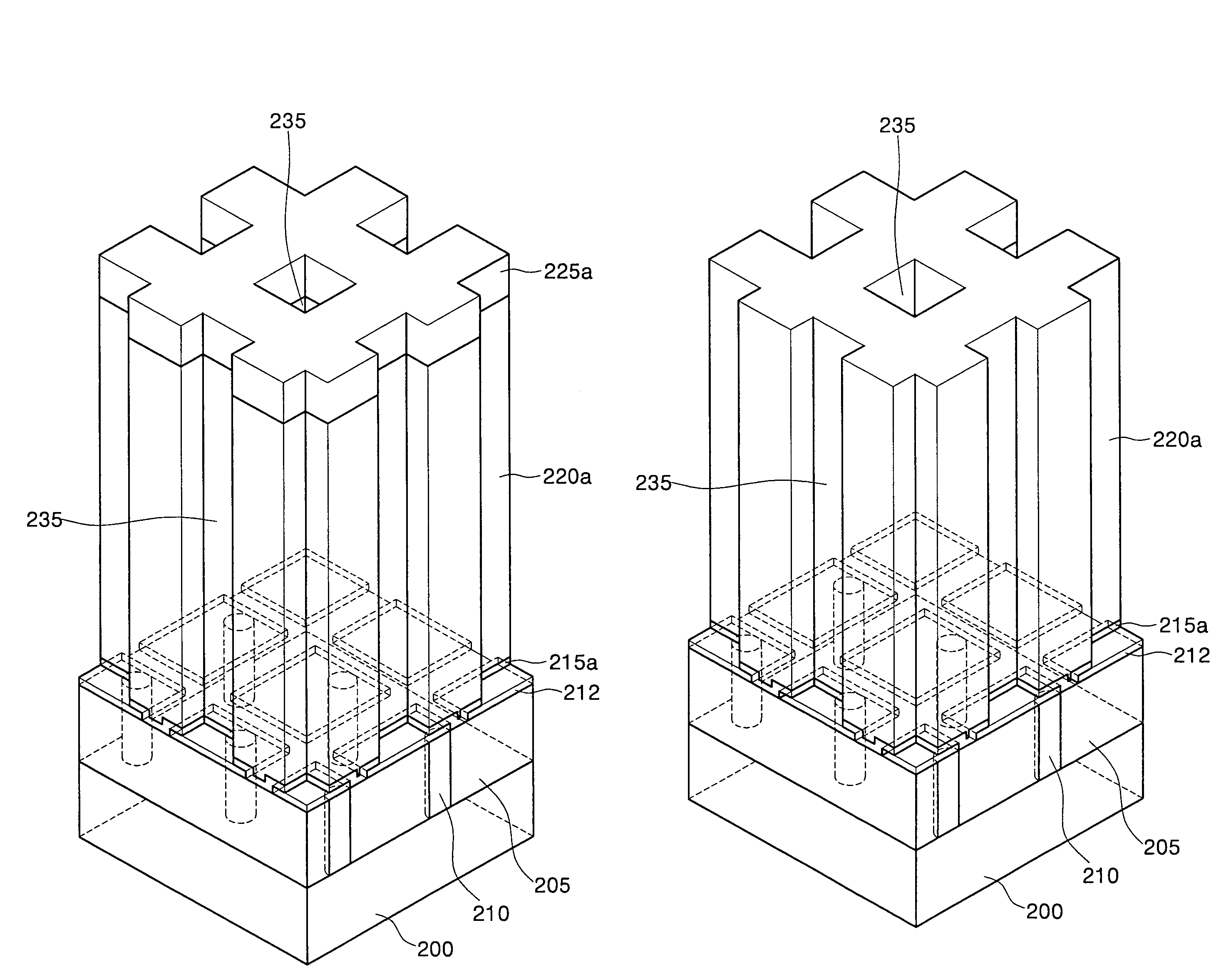
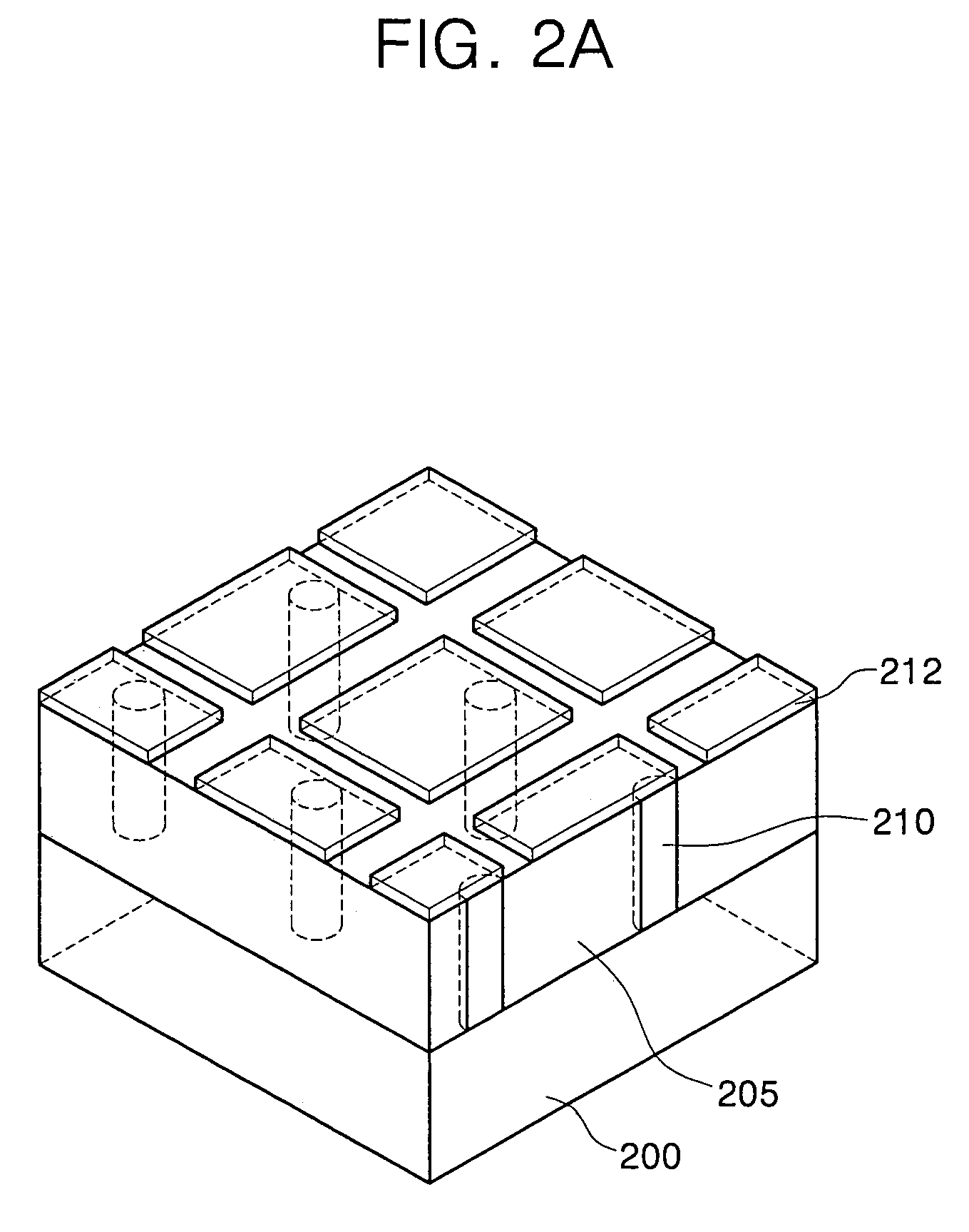
[0049]Referring to FIG. 2A, an interlayer insulating layer 205 is formed on a semiconductor substrate 200. The interlayer insulating layer 205 may be formed of an oxide layer, BPSG (borophosphosilicate glass) or PSG (phosphosilicate glass). Buried contact plugs 210 are formed to penetrate the interlayer insulating layer 205. The buried contact plugs 210 may comprise polysilicon. The buried contact plugs 210 have the same height as the thickness of the interlayer insulating layer 205. Beneficially, a buffer conductive layer is formed on the semiconductor substrate 200 having the buried contact plugs 210 formed thereon. The buffer conductive layer may comprise polysilicon. The buffer conductive layer is patterned, thereby forming buffer conductive layer patterns 212 being in contact with the buried contact plugs 210 respective...

second embodiment

[0063]FIGS. 3A to 3E are perspective views illustrating a method of fabricating a semiconductor device having box-shaped cylindrical storage nodes according to a

[0064]Referring to FIG. 3A, an interlayer insulating layer 305 is formed on a semiconductor substrate 300 as described in reference to FIGS. 2A and 2B. Buried contact plugs 310 are formed to penetrate the interlayer insulating layer 305. Buffer conductive layer patterns 312 are formed on the semiconductor substrate 300 having the buried contact plugs 310 formed thereon, and the buffer conductive layer patterns 312 are in contact with the buried contact plugs 310 respectively, and have a greater width than the buried contact plugs 310. The buffer conductive layer patterns 312 may comprise polysilicon. An etch stop layer 315 may be formed on the semiconductor substrate 300 having the buffer conductive layer patterns 312 formed thereon. The etch stop layer 315 may be formed of a silicon nitride layer. A molding layer 320 is for...

third embodiment

[0071]FIGS. 4A to 4E are perspective views illustrating a method of fabricating a semiconductor device having box-shaped cylindrical storage nodes according to a

[0072]Referring to FIG. 4A, an interlayer insulating layer 405 is formed on a semiconductor substrate 400 as described in reference to FIGS. 2A and 2B. The interlayer insulating layer 405 may be formed of an oxide layer, BPSG, or PSG. Buried contact plugs 410 are formed to penetrate the interlayer insulating layer 405. The buried contact plugs 410 may comprise polysilicon. The buried contact plugs 410 have the same height as the thickness of the interlayer insulating layer 405. Beneficially, buffer conductive layer patterns 412 are formed on the semiconductor substrate 400 having the buried contact plugs 410 formed thereon, the buffer conductive layer patterns 412 each being in contact with respective ones of the buried contact plugs 410, and having a greater width than the buried contact plugs 410. The buffer conductive lay...


PUM


Abstract

A method of forming box-shaped cylindrical storage nodes includes forming an interlayer insulating layer on a semiconductor substrate. Buried contact plugs are formed to penetrate the interlayer insulating layer. A molding layer and a photoresist layer are then sequentially formed on the substrate. Using a first phase shift mask having line-and-space patterns, the photoresist layer is exposed, forming first exposure regions. Using a second phase shift mask having line-and-space patterns, the photoresist layer is exposed again, forming second exposure regions intersecting the first exposure regions. The photoresist layer is then developed, forming a photoresist pattern having rectangular-shaped openings formed at intersections of the first and the second exposure regions. The molding layer is etched using the photoresist pattern as an etch mask, forming storage node holes exposing the buried contact plugs. Storage nodes are formed inside the storage node holes.

Description

CROSS REFERENCES TO RELATED APPLICATIONS[0001]This application claims priority under 35 U.S.C. § 119 from Korean Patent Application No. 2004-47895, filed on Jun. 24, 2004, the contents of which are hereby incorporated by reference in their entirety for all purposes as if fully set forth herein.BACKGROUND AND SUMMARY[0002]1. Technical Field[0003]The present invention relates to a semiconductor device and a fabrication method thereof, and more particularly, to a semiconductor device having box-shaped cylindrical storage nodes and a method of fabricating the same.[0004]2. Description of the Related Art[0005]A semiconductor memory device, particularly, a dynamic random access memory (DRAM) device is a memory device for storing data in a unit cell. That is, the unit cell of such a DRAM includes one access transistor and one cell capacitor, which are connected in series. As the integration of such a DRAM is increased, the area of the unit cell is significantly reduced, and thus, the capac...

Claims


Application Information

Patent Timeline
Patent Type & Authority Patents(United States)
IPC IPC(8): H01L21/8242H01L21/20H01L21/76H01L21/02H01L27/108
CPCH01L27/10852H01L28/91H01L21/76816H10B12/033H10B99/00
Inventor KIM, SANG-HO
Owner SAMSUNG ELECTRONICS CO LTD
Why Eureka
Try Eureka