System and method for modeling an integrated circuit system

a modeling system and integrated circuit technology, applied in the field of semiconductor devices, can solve problems such as inability to make predictions about circuit elements fabricated using a different process, inability to meet the efficiency and accuracy of known modeling methods, and inability to model circuit elements. to achieve the effect of reducing disadvantages or greatly reducing problems

Active Publication Date: 2007-10-09
TEXAS INSTR INC
View PDF11 Cites 8 Cited by
  • Summary
  • Abstract
  • Description
  • Claims
  • Application Information

AI Technical Summary

Benefits of technology

[0008]In accordance with the present invention, a system and method for modeling an integrated circuit package is provided that substantially eliminates or greatly reduces disadvantages and problems associated with conventional techniques.
[0011]Certain examples of the invention may provide one or more technical advantages. A technical advantage of particular embodiments of the present invention is a system and method for modeling and simulating a proposed design of an integrated circuit system analyzing different package configurations in context with microchip parasitics, microchip power supply noise, and a printed circuit board netlist. Accordingly, the analysis may be done in the architectural stage of design to support a “reliability test design”. The reliability test design is a version of the package design that is used for mechanical stress testing. The reliability testing and the IC design are accomplished in parallel which in turn requires the package configuration to be committed early in the design. The analysis allows for improved choices for performance and costs to be made early in the process, to avoid an impact on the overall design schedule.
[0012]Another technical advantage of the particular embodiments of the present invention include a modeling and simulation analysis that is based upon physical parameters that can be modified as different package types are explored and different corner conditions are explored. Thus, the efficiency of the model and analysis is increased, and allows a design team to make running multiple simulations using current simulation tool, more practical.

Problems solved by technology

Modeling circuits is problematic when the characteristics of the individual circuit elements are not known.
Known methods for modeling such circuit elements, however, have not been completely satisfactory with respect to efficiency and accuracy.
A problem with this method is that it cannot be used to make predictions about circuit elements fabricated using a different process.
Prior models generated using these simulators, however, were not sufficiently accurate.
While these approaches have provided improvements over prior approaches, the challenges in the field of circuit fabrication has continued to increase with demands for more and better techniques having greater efficiency and accuracy.
Design and analysis of integrated circuit systems including the chip, package and printed circuit board, becomes more complex as the size of the system is reduced, and the number of components and complexity increases.
Unfortunately, accurate modeling of integrated circuit packages by known methods require that the design of many components be substantially complete, in order to account for their effect on the operation of the system.
Both of these processes generate netlists that are too large to be practical for doing multiple simulations and evaluating alternatives.
The design of such systems takes a significant amount of time and resources, that may be lost if the results of the analysis are unfavorable.
Moreover, accurate modeling by known methods apply to small portions of the design, but are impossible to perform on the entire design, based upon the amount of data and number of calculations required of the particular analysis tool(s).

Method used


Image

  • System and method for modeling an integrated circuit system
  • System and method for modeling an integrated circuit system
  • System and method for modeling an integrated circuit system

Examples


Embodiment Construction

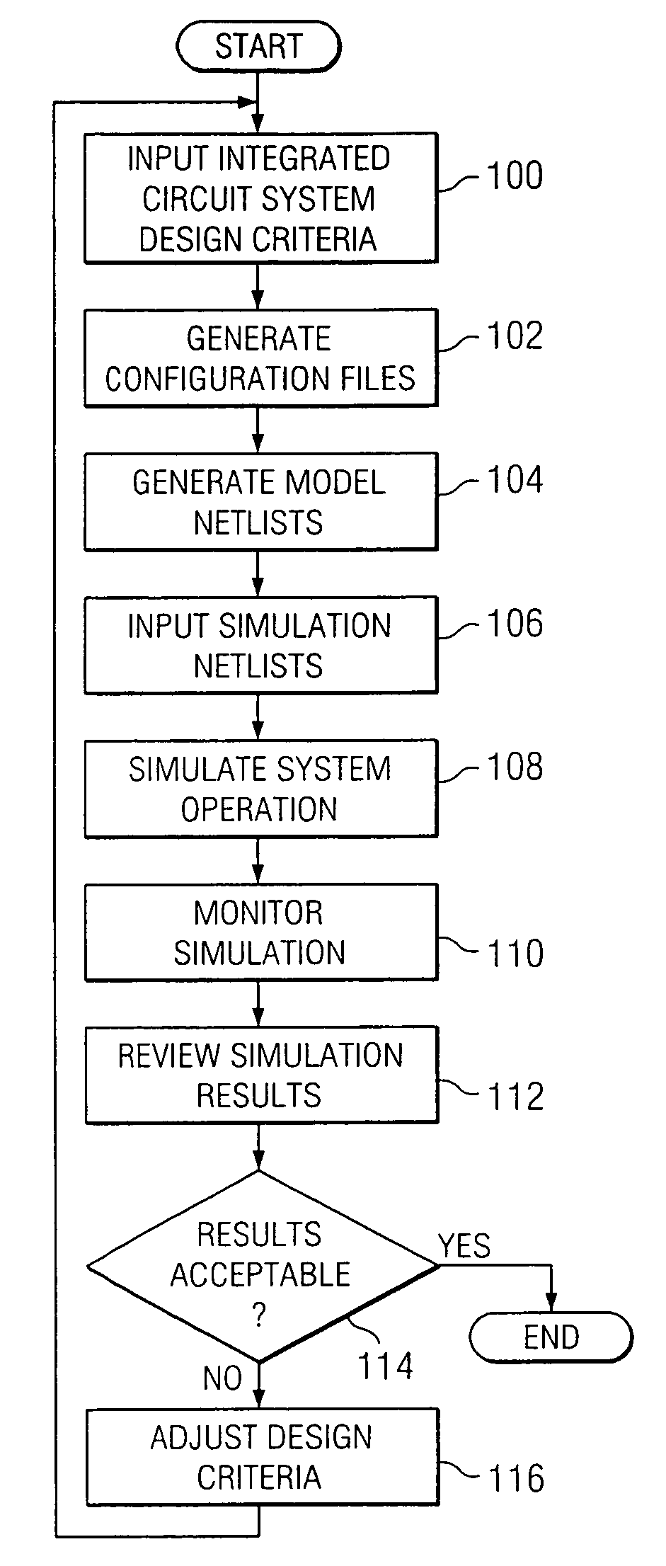
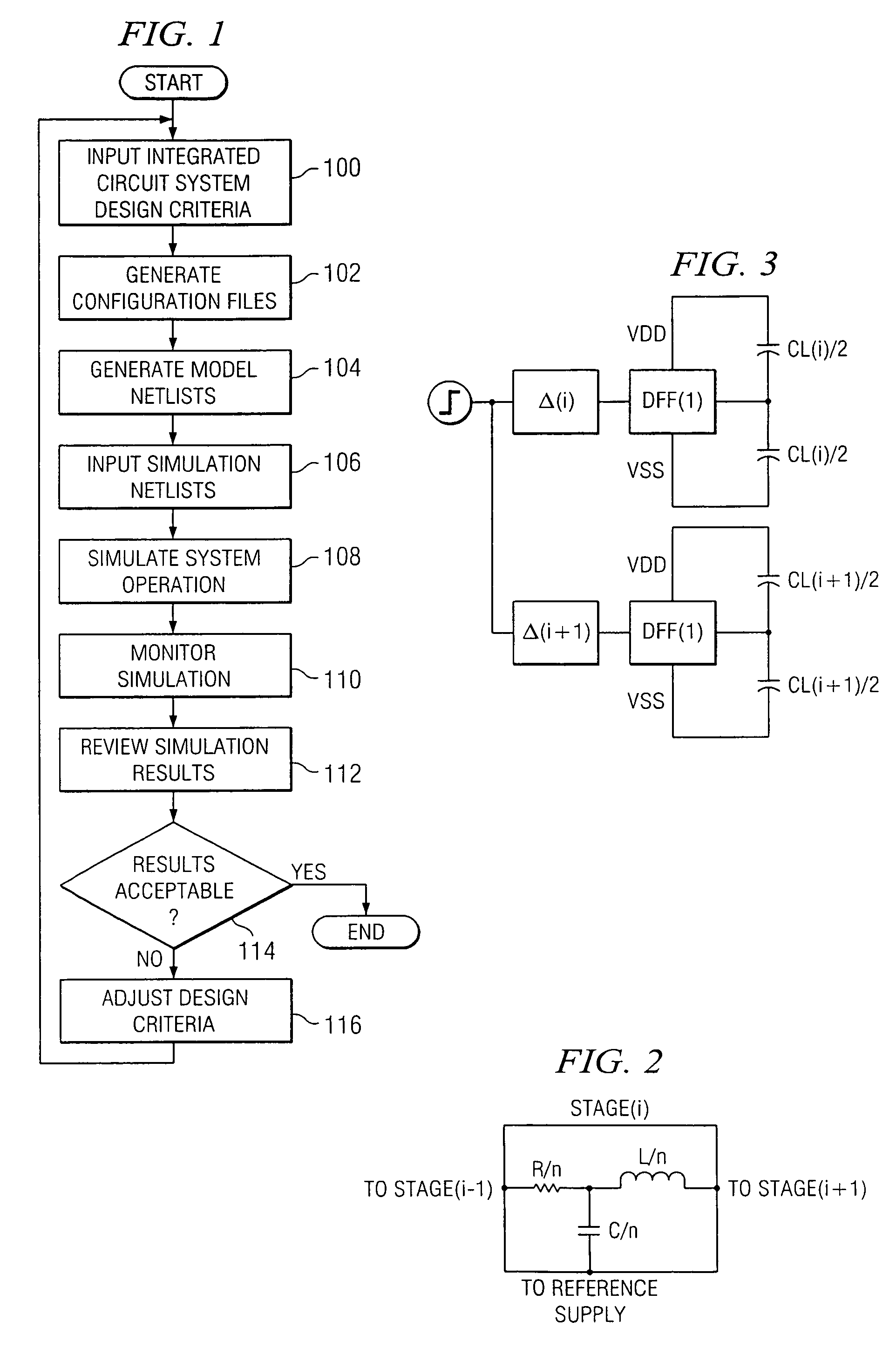
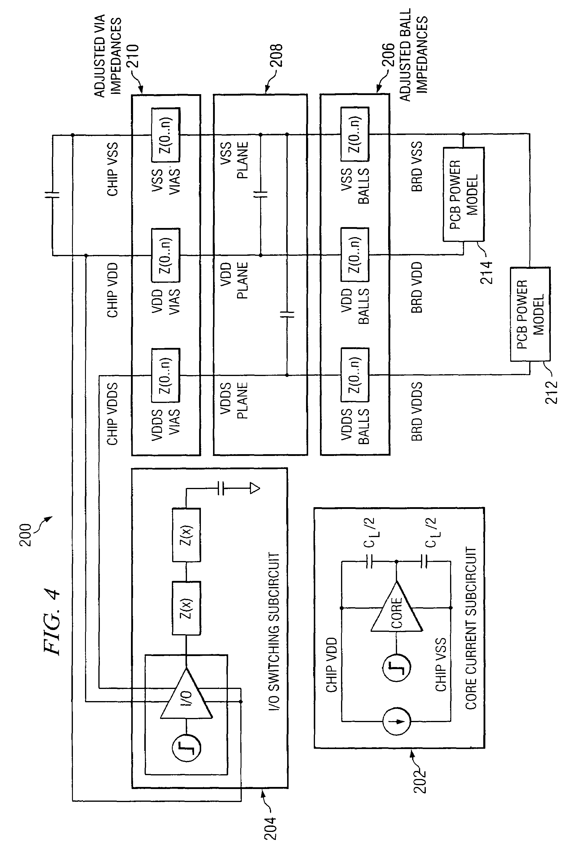
[0019]An embodiment of the present invention and its advantages are best understood by referring to FIGS. 1-4 of the drawings, like numerals being used for like and corresponding parts of the various drawings.

[0020]FIG. 1 illustrates a method for modeling a system that includes a microchip, a package and a printed circuit board (PCB). The method of FIG. 1 may be used to analyze the electrical characteristics of power switching noise associated with a particular design, for example a multimillion-gate design, on the package and PCB. The modeling and simulation can be done at the architectural stage of the design to enable designers to consider tradeoffs (e.g., cost versus performance) of different package configurations. The electrical analysis may be used to determine instantaneous IR and L di / dt drop that is anticipated at the chip power connections through the package and printed circuit board. In Mixed Signal designs, the frequency and magnitude of the instantaneous voltage drop ...


PUM


Abstract

The teachings of the present invention provide a method for modeling an integrated circuit system including a microchip, an integrated circuit package, and a printed circuit board. The method includes generating a configuration file including parasitics regarding ball grid arrays and vias intended for use in design of the integrated circuit system. A netlist may be generated using the configuration file. In accordance with a particular embodiment of the present invention, the operation of the integrated circuit system may be simulated to determine anticipated operating characteristics of the integrated circuit system.

Description

RELATED APPLICATIONS[0001]This application claims the benefit of U.S. Provisional Patent Application Ser. No. 60 / 605,867, filed on Aug. 31, 2004, and currently pending.FIELD OF INVENTION[0002]The present invention relates generally to semiconductor devices and more particularly to a system and method for modeling an integrated circuit system.BACKGROUND OF THE INVENTION[0003]Designing circuits that are used in products such as digital signal processors requires making predictions of how the individual circuit elements, such as transistors, will behave. Modeling individual circuit elements requires making predictions of how the fabrication process affects the behavior of the resulting circuit elements. By making predictions, circuit designers can understand how the circuit will operate without the time and expense of actually building the circuit. Modeling circuits is problematic when the characteristics of the individual circuit elements are not known. Known methods for modeling such...

Claims


Application Information

Patent Timeline
Patent Type & Authority Patents(United States)
IPC IPC(8): G06F17/50H03K17/693
CPCG06F17/5036G06F30/367
Inventor KIEL, STEPHEN N.SINHA, SNEHAMAYHOWARD, GREGORY E.
Owner TEXAS INSTR INC
Why Eureka
Try Eureka