Packaged device and method of forming same

a technology of integrated circuits and packaging devices, which is applied in the direction of semiconductor devices, semiconductor/solid-state device details, electrical equipment, etc., can solve the problems of expensive and time-consuming to form leadframes and package devices

Inactive Publication Date: 2007-10-23
TAIWAN SEMICON MFG CO LTD
View PDF12 Cites 80 Cited by
  • Summary
  • Abstract
  • Description
  • Claims
  • Application Information

AI Technical Summary

Problems solved by technology

However, it can be expensive and time-consuming to form a leadframe and package a device if steps like chemical etching and etch back are required.

Method used


Image

  • Packaged device and method of forming same
  • Packaged device and method of forming same
  • Packaged device and method of forming same

Examples


Embodiment Construction

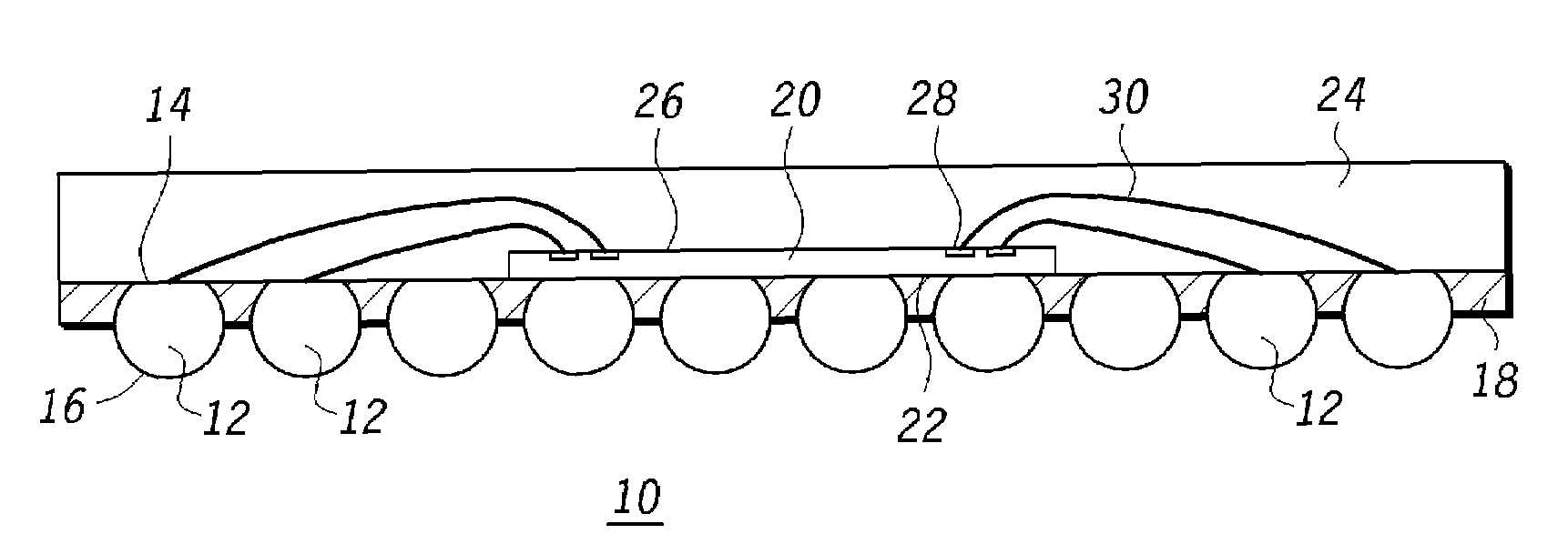
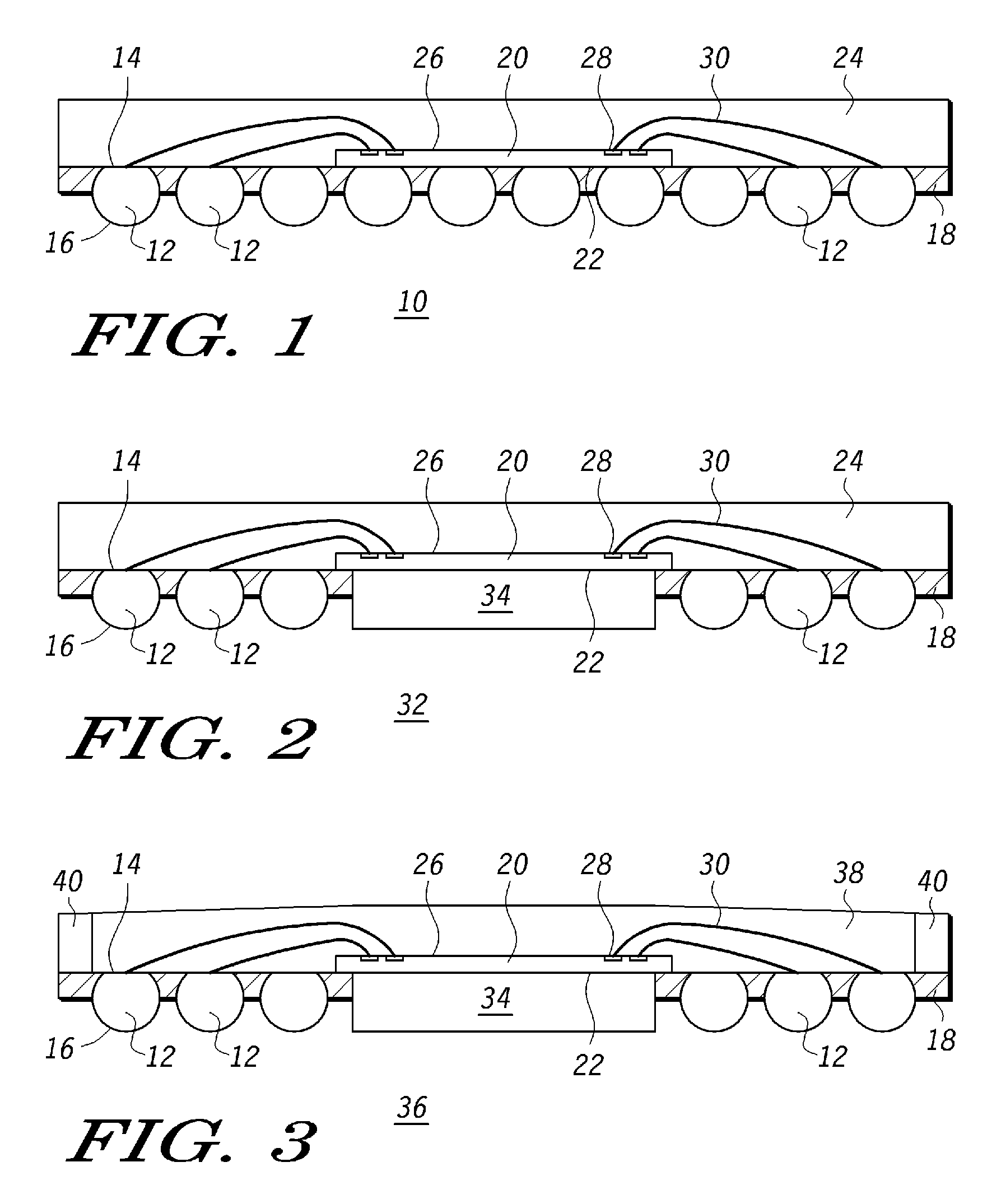
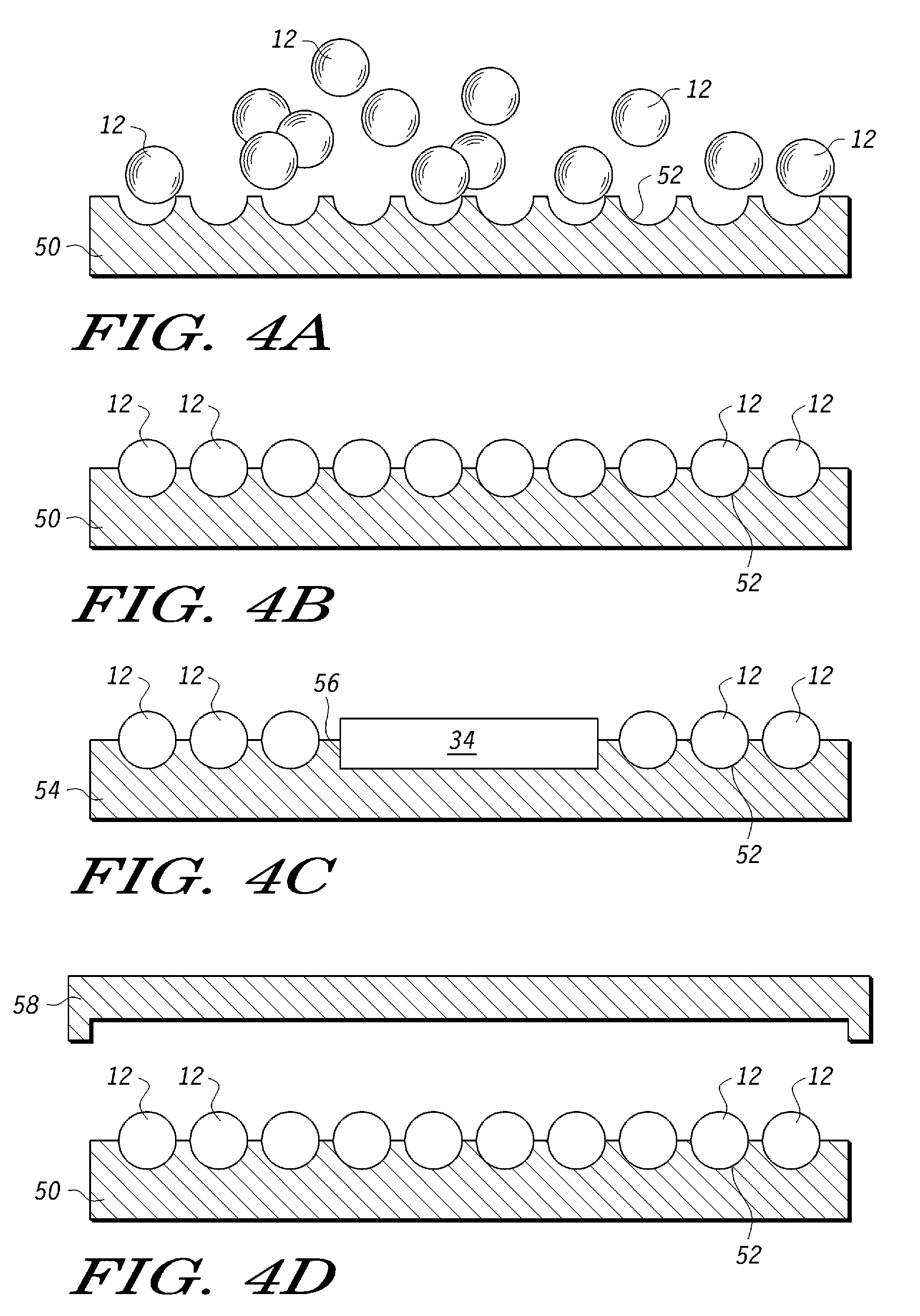
[0011]The detailed description set forth below in connection with the appended drawings is intended as a description of the presently preferred embodiments of the invention, and is not intended to represent the only form in which the present invention may be practiced. It is to be understood that the same or equivalent functions may be accomplished by different embodiments that are intended to be encompassed within the spirit and scope of the invention. Further, it will be understood by those of skill in the art that the drawings have been simplified and are not drawn to scale.

[0012]The present invention provides a method of packaging an integrated circuit die, including the steps of:

[0013]loading a plurality of conductive balls into recesses formed in a platen;

[0014]transferring the platen to a cavity of a first part of a mold;

[0015]pressing a second part of the mold against the conductive balls, thereby at least partially flattening a top surface of the conductive balls;

[0016]inje...


PUM


Abstract

A method of packaging an integrated circuit die (12) includes the steps of loading an array of soft conductive balls into recesses formed in a platen and locating the platen in a first part of a mold cavity. A second part of the mold is pressed against the balls to flatten a surface of the balls. A first mold compound then is injected into the mold cavity such that the mold compound surrounds exposed portions of the balls. The balls are removed from the platen and a first side of an integrated circuit die is attached to the balls such that the die is surrounded by the balls. Die bonding pads on a second side of the die are electrically connected to respective ones of the balls surrounding the die, and then the die, the electrical connections, and a top portion of the conductive balls is encapsulated with a second mold compound. The result is an encapsulated IC having a bottom side with exposed balls.

Description

CROSS REFERENCE TO RELATED APPLICATIONS[0001]This application is a divisional application of U.S. application Ser. No. 11 / 191,132 filed Jul. 27, 2005 now U.S. Pat. No. 7,179,682.BACKGROUND OF THE INVENTION[0002]The present invention relates to integrated circuit packaging, and more particularly to an improved process for fabricating a Ball Grid Array (BGA) packaged device.[0003]An integrated circuit (IC) die is a small device formed on a semiconductor wafer, such as a silicon wafer. A leadframe is a metal frame that usually includes a paddle that supports the IC die that has been cut from the wafer. The leadframe also has lead fingers that provide external electrical connections. That is, the die is attached to the die paddle and then bonding pads of the die are connected to the lead fingers via wire bonding or flip chip bumping to provide the external electrical connections. Encapsulating the die and wire bonds or flip chip bumps with a protective material forms a package. Dependin...

Claims


Application Information

Patent Timeline
Patent Type & Authority Patents(United States)
IPC IPC(8): H01L23/48
CPCH01L21/486H01L21/565H01L23/3128H01L23/49816H01L23/49861H01L24/97H01L2924/10253H01L2924/01028H01L2924/01076H01L2924/01033H01L2924/01006H01L24/48H01L2924/15311H01L2924/14H01L2924/01082H01L2924/01079H01L2924/01078H01L2924/0105H01L2924/01047H01L2924/01046H01L2924/01029H01L2924/0102H01L2924/01014H01L2224/45124H01L2224/45144H01L2224/45147H01L2224/48091H01L2224/97H01L2924/01004H01L2924/01012H01L2924/01013H01L2924/00014H01L2224/85H01L2924/00H01L24/45H01L2224/45015H01L2224/45139H01L2224/45164H01L2224/45169H01L2224/45565H01L2924/181H01L2924/18165H01L2924/00012H01L2924/20751H01L2924/20752H01L2924/20753H01L2924/20754H01L2224/4569H01L2924/20755H01L2224/43848
Inventor FOONG, CHEE SENG
Owner TAIWAN SEMICON MFG CO LTD
Why Eureka
Try Eureka