Semiconductor device capable of suppressing current concentration in pad and its manufacture method

a semiconductor and pad technology, applied in semiconductor devices, semiconductor/solid-state device details, electrical devices, etc., can solve the problems of reducing tight adhesion and the method of forming wiring by partially etching a metal layer is nowadays associated with some technical limit, so as to avoid excessive current concentration and suppress the formation of a depressed upper surface

Inactive Publication Date: 2008-01-01
FUJITSU SEMICON LTD
View PDF7 Cites 34 Cited by
  • Summary
  • Abstract
  • Description
  • Claims
  • Application Information

AI Technical Summary

Benefits of technology

[0022]It is an object of the present invention to provide a semiconductor device having a pad structure capable of suppressing excessive current concentration in a pad and its manufacture method.
[0023]It is another object of the present invention to provide a semiconductor device having a pad structure capable of mitigating instability of contact between a pad and an inspection probe and its manufacture method.
[0026]Since a plurality of convex regions are left in the pad part of the recess, it is possible to suppress the formation of a depressed upper surface of the first film in the pad part, when the first film is etched at the step (e). Since the recess area ratio in the near wiring area is relatively large, the first pad area ratio in the near wiring area becomes large. It is therefore possible to avoid excessive current concentration in a particular area in the first pad when current is flowed from the wiring to the pad.

Problems solved by technology

A method of forming wiring by partially etching a metal layer is nowadays associated with some technical limit.
The silicon oxide film doped with fluorine and absorbed moisture may generate gas at a succeeding heat treatment process or may cause a lower tight adhesion.
If the lower insulating film is made of insulating organic material such as polyallyl ether, in addition to moisture absorption and lowered tight adhesion, the following problem arises.

Method used


Image

  • Semiconductor device capable of suppressing current concentration in pad and its manufacture method
  • Semiconductor device capable of suppressing current concentration in pad and its manufacture method
  • Semiconductor device capable of suppressing current concentration in pad and its manufacture method

Examples


first embodiment

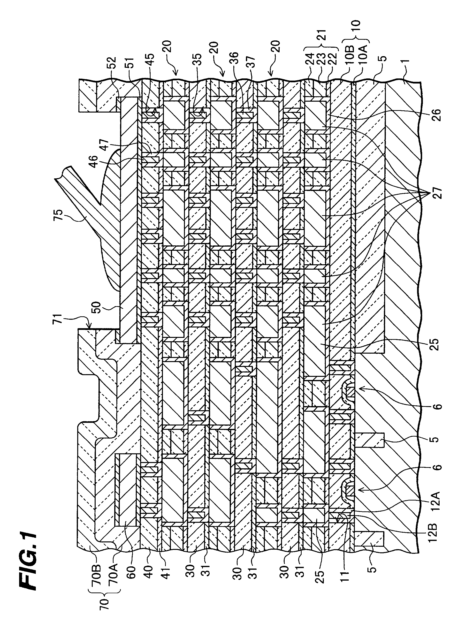
[0040]FIG. 1 is a cross sectional view of a semiconductor device according to the invention. In the surface layer of a semiconductor substrate 1, an element separation insulating film 5 is formed which defines active regions. The element separation insulating film 5 is made of local oxidation of silicon (LOCOS) or shallow trench isolation (STI). A MOS field effect transistor (MOSFET) 6 is formed on the surface of the active region.

[0041]An interlayer insulating film 10 is formed on the semiconductor substrate 1, covering MOSFET 6. The interlayer insulating film 10 has a two-layer structure of a lower layer 10A made of silicon nitride and an upper layer 10B made of silicon oxide. Via holes 11 are formed through the interlayer insulating film 10. The via holes 11 are formed in the areas corresponding to the source / drain regions of MOSFET 6. The inner surface of the via hole 11 is covered with a barrier layer 12A made of titanium nitride (TiN), and a conductive plug 12B made of tungste...

second embodiment

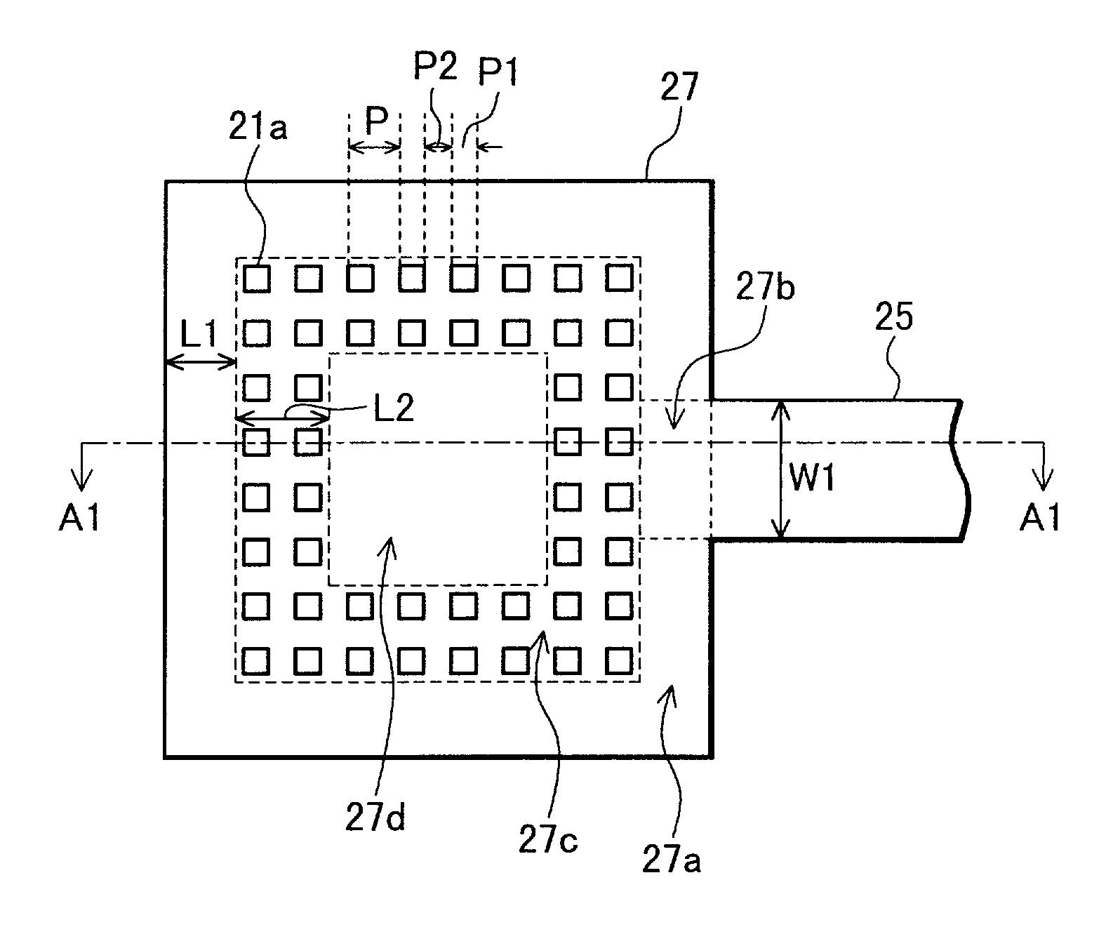
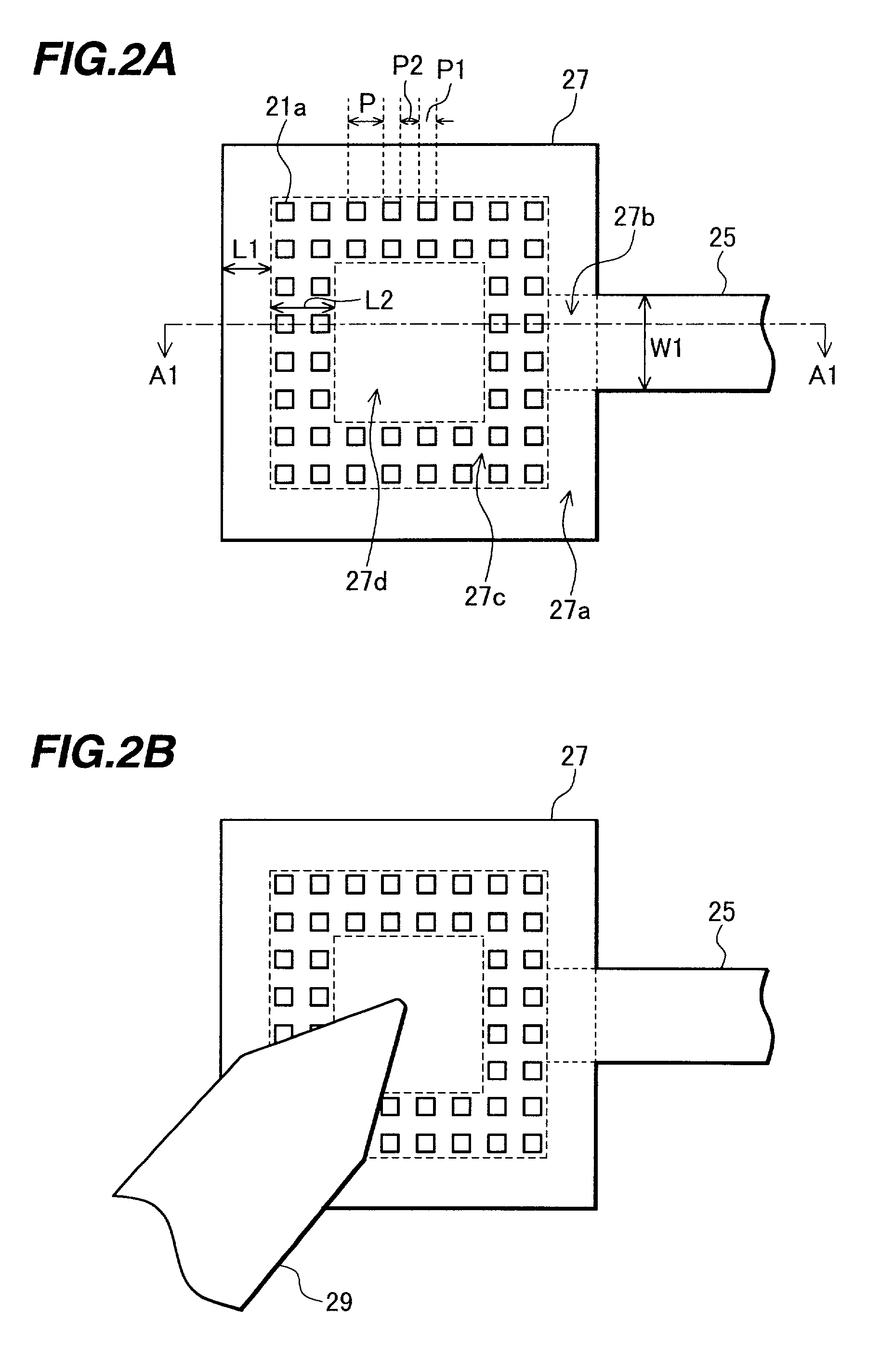
[0096]A first wiring layer 20 is formed on the interlayer insulating film 10. The intra-layer insulating film 21 in the first wiring layer 20 shown in FIG. 1 has the three-layer structure of the etching stopper film 22, layer 23 of silicon oxide doped with fluorine and silicon oxide layer 24. An intra-layer insulating film 21 of the semiconductor device of the second embodiment has a two-layer structure of an etching stopper film of silicon nitride and a silicon oxide layer. A pad 27 is filled in a recess formed in the intra-layer insulating film 21. A barrier metal layer 26 is disposed between the inner surface of the recess and the pad 27.

[0097]On the first wiring layer 20, a first etching stopper film 100, an interlayer insulating film 101, a second etching stopper film 102, and an intra-layer insulating film 103 are sequentially formed. Each of the first and second etching stopper films 100 and 102 is made of silicon nitride and has a thickness of 50 nm. Each of the interlayer i...


PUM


Abstract

An interlayer insulating film is formed on a semiconductor substrate. An intra-layer insulating film is formed on the interlayer film. A recess is formed through the intra-layer film. The recess has a pad-part and a wiring-part continuous with the pad-part. The pad-part is wider than the width of the wiring-part. Convex regions are left in the pad-part. The convex regions are disposed in such a manner that a recess area ratio in a near wiring area superposed upon an extended area of the wiring-part into the pad-part, within a first frame area having as an outer periphery an outer periphery of the pad-part and having a first width, becomes larger than a recess area ratio in a second frame area having as an outer periphery an inner periphery of the first frame area and having a second width. A conductive film is filled in the recess.

Description

CROSS REFERENCE TO RELATED APPLICATION[0001]This application is based on Japanese patent application 2001-271416, filed on Sep. 7, 2001, the whole contents of which are incorporated herein by reference.BACKGROUND OF THE INVENTION[0002]A) Field of the Invention[0003]The present invention relates to a semiconductor device and its manufacture method, and more particularly to a semiconductor device manufacture method capable of preventing a lower manufacture yield when wiring and pads are formed by a damascene method and to a semiconductor device having a structure suitable for the manufacture method.[0004]B) Description of the Related Art[0005]Design rules of multi-layer wiring structures are becoming smaller as the degree of integration and micro patterning of semiconductor integrated circuit devices (LSI) becomes higher. A method of forming wiring by partially etching a metal layer is nowadays associated with some technical limit. In order to solve this problem, a damascene method is...

Claims


Application Information

Patent Timeline
Patent Type & Authority Patents(United States)
IPC IPC(8): H01L29/00H01L23/52H01L21/3205H01L21/60H01L21/768H01L23/485
CPCH01L21/76801H01L21/76802H01L21/76808H01L24/03H01L24/05H01L24/48H01L24/85H01L2924/05042H01L2924/13091H01L2924/14H01L2224/02126H01L2224/0401H01L2224/04042H01L2224/05006H01L2224/05073H01L2224/05093H01L2224/05095H01L2224/05187H01L2224/05546H01L2224/05624H01L2224/05647H01L2224/48463H01L2224/85H01L2924/01002H01L2924/01004H01L2924/01005H01L2924/01006H01L2924/01014H01L2924/01015H01L2924/01018H01L2924/01022H01L2924/01029H01L2924/01033H01L2924/01038H01L2924/0105H01L2924/01073H01L2924/01074H01L2924/01078H01L2924/01082H01L2924/04941H01L2924/04953H01L2924/00014H01L2224/48453H01L2224/02166H01L2924/1306H01L2924/01013H01L2224/78H01L2224/45099H01L2924/00H01L21/3205
Inventor WATANABE, KENICHI
Owner FUJITSU SEMICON LTD
Why Eureka
Try Eureka