Method and system for managing design corrections for optical and process effects based on feature tolerances

a technology of feature tolerances and design corrections, applied in the field of fabricating integrated circuits, can solve the problems of affecting the process, difficult for the projection lens to reproduce the high spatial frequency components, and complex interaction of the electric fields of adjacent objects, so as to avoid post-correction compaction and sacrifice accuracy.

Active Publication Date: 2008-02-26
CADENCE DESIGN SYST INC
View PDF10 Cites 174 Cited by
  • Summary
  • Abstract
  • Description
  • Claims
  • Application Information

AI Technical Summary

Benefits of technology

[0035]The advantage of this method is that the layout flattening is controlled during the OPC process. At each instance, the suitability of the corrections is determined, and if the corrections are deemed unsuitable, new instances are created, as necessary. This avoids the requirement for post OPC compaction and trying to rebuild the hierarchy after OPC has been performed for the entire design.

Problems solved by technology

Thus, it may be difficult for the projection lens to reproduce the high spatial frequency components required to reproduce the sharp edges or corners in polygon objects for example.
Also, light entering a mask opening from one object may impact another shape in close proximity, leading to a complex interaction of the electric fields of adjacent objects.
Thus, the final shapes that are produced on the wafer will often have rounded corners and may bulge towards adjacent objects in ways that can impact the process yield.
This resulting image distortion, called optical proximity effect, is responsible for the most significant distortion that arises in the transfer of the mask pattern onto the wafer.
One issue is how the OPC, RET, and / or process corrections should be applied to repeating patterns such as instances of a cell in a hierarchical pattern description, such as in a structure reference or an array reference.
However a result of this correction approach is that the lithography data are severely flattened relative to the layout data since different instantiations for the same repeating pattern from the target layout are required in the lithography data.

Method used


Image

  • Method and system for managing design corrections for optical and process effects based on feature tolerances
  • Method and system for managing design corrections for optical and process effects based on feature tolerances
  • Method and system for managing design corrections for optical and process effects based on feature tolerances

Examples


Embodiment Construction

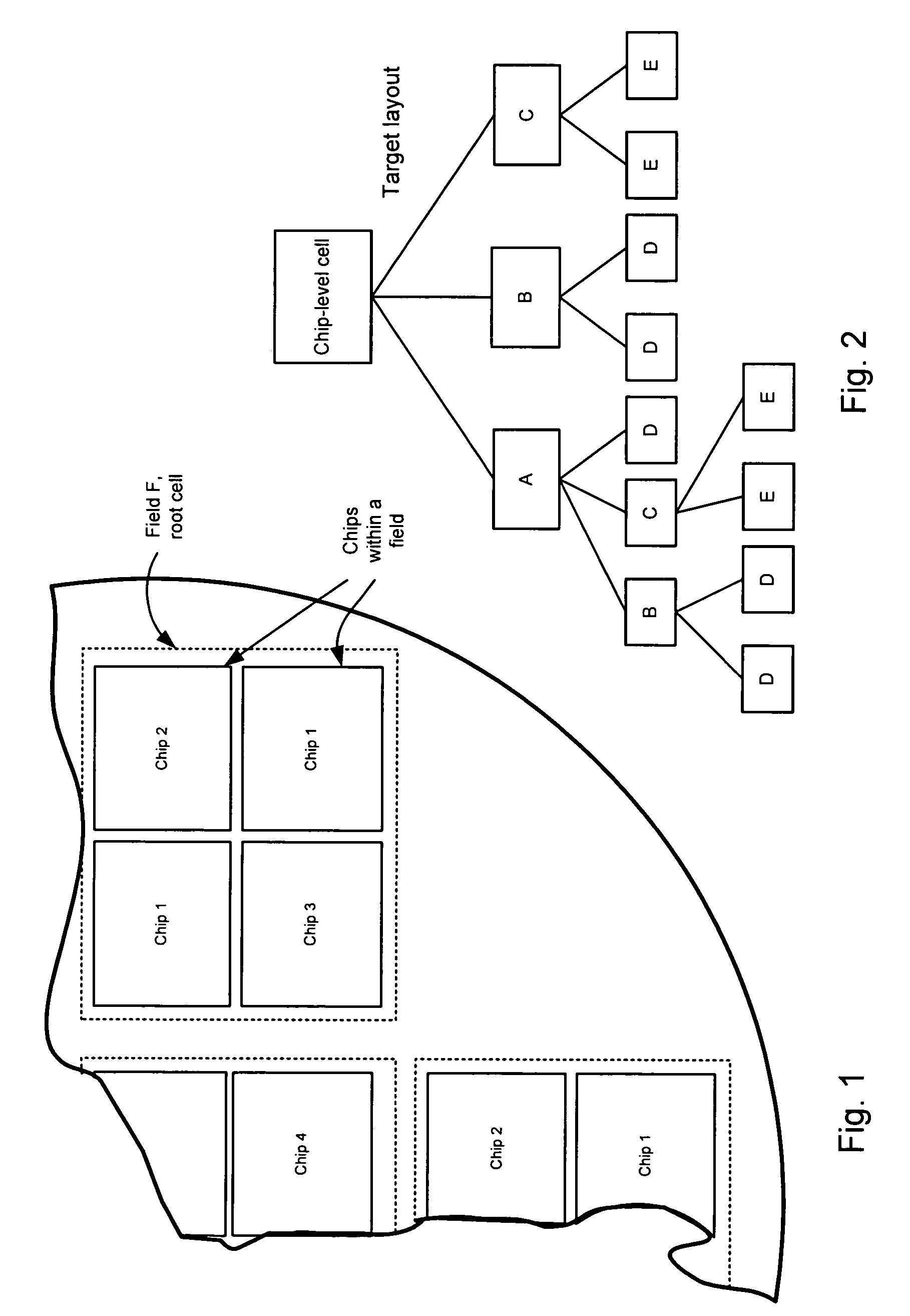
[0052]FIG. 1 illustrates the schematic arrangement of multiple chips within a field and the multiple exposures of the field across a wafer.

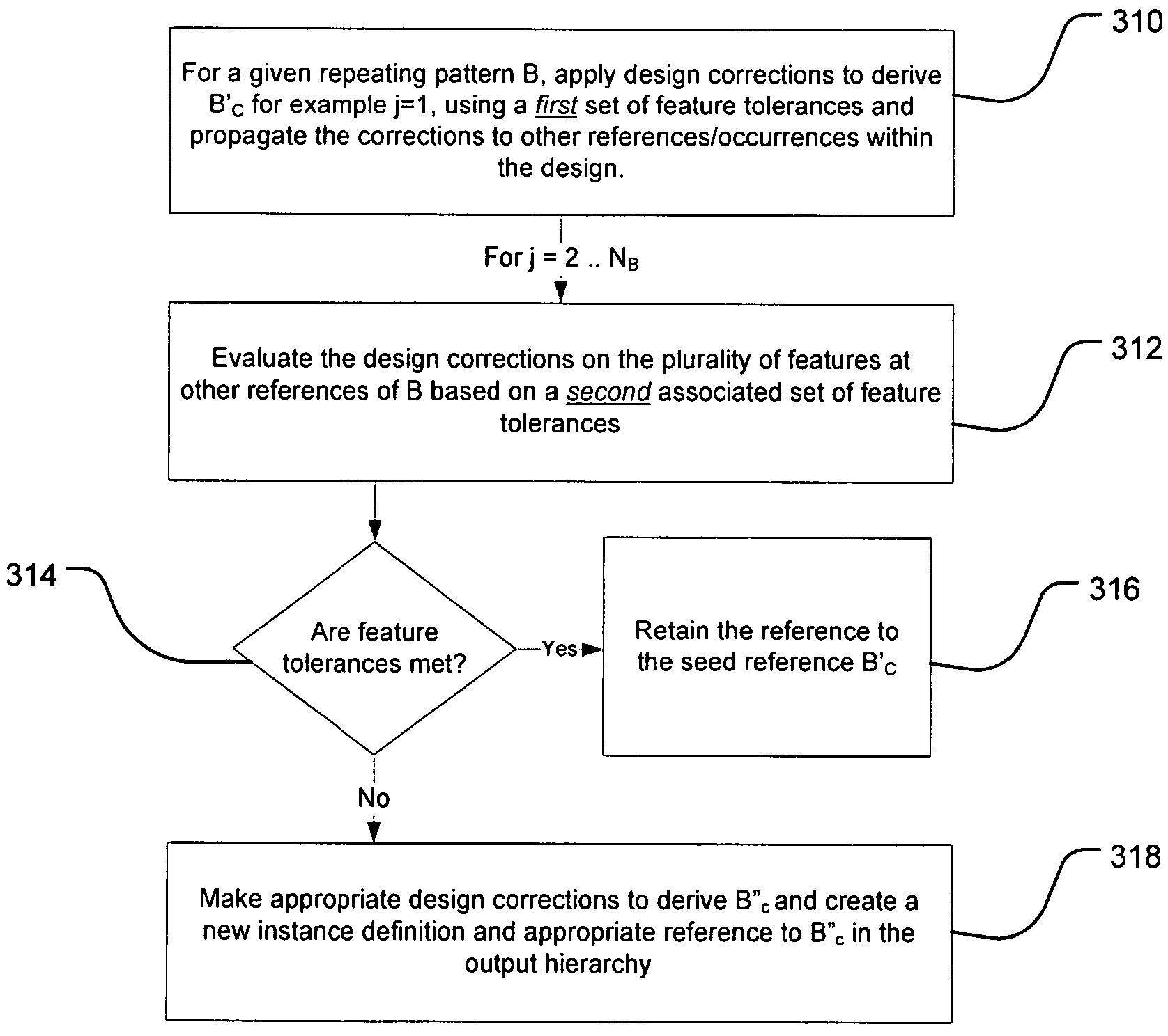
[0053]Specifically, in the design, the root cell often exists at the level of the chip or field F. Within the field there may be multiple placements of chips or functional structures within chips such as chip-level cells Chip 1, Chip 2, Chip 3. Within each of these child cells Chip 1, Chip 2, Chip 3 are repeating patterns. These repeating patterns are often repeated many times within each chip Chip 1, Chip 2, Chip 3 at different coordinates. The patterns are often also rotated, reflected, and possibly scaled at each placement. In one case, the repeating patterns are consolidated across the field for a field wide correction based on tolerances. In another aspect, corrections are incorporated within a single chip based on field position and propagated to other chips within the field, which contain the same repeating patterns and their suitability v...


PUM


Abstract

A method for modifying instances of a repeating pattern in an integrated circuit design to correct for perturbations during rendering is described. In the typical embodiment, these corrections are optical proximity corrections that correct for optical effects during the projection of the mask pattern onto the wafer and / or processing effects for example photoresist response and etching effects. The method comprises determining a correction for the repeating pattern based on a first set of tolerances for features of the repeating pattern. Then, the suitability of the corrections is evaluated for instances of the repeating pattern in the integrated circuit design based on a second set of tolerances, which is different from the first set of tolerances. This can be used to preserve much of the hierarchy of the layout data in the corrected, or lithography, data. This can be achieved during the OPC process, thus avoiding the post OPC compaction. It can further take advantage of the fact that, for a given physical layer of a chip for example, different portions of the representing design polygons typically have different requirements on pattern fidelity on the wafer while perturbations may vary as a function of field position. By applying knowledge of the feature tolerances, and allowing design corrections only when tolerances are not met, the data explosion that occurs when moving from layout to lithography data can be contained without sacrificing accuracy.

Description

BACKGROUND OF THE INVENTION[0001]The process of fabricating integrated circuits typically involves a functional design step, followed by a physical design step. During the functional design step, a design concept is described using a hardware description language and is then converted into a netlist, which specifies the electronic components and the connections between the components. The physical design step specifies the placement of the electrical components or elements on the chip and routing of the connections between the electrical components thereby implementing the netlist. The physical design process generates the physical design data, which are synonymously called layout data, layout, or target layout.[0002]The target layout defines a set of binary patterns or objects, which are also called “features” or “geometric features”. Usually the objects are represented as a polygon or collection of polygons in the layout data in order to facilitate the specification of the objects...

Claims


Application Information

Patent Timeline
Patent Type & Authority Patents(United States)
IPC IPC(8): G06F17/50
CPCG06F17/5068G06F30/39
Inventor KAMAT, VISHNU GOVIND
Owner CADENCE DESIGN SYST INC
Why Eureka
Try Eureka