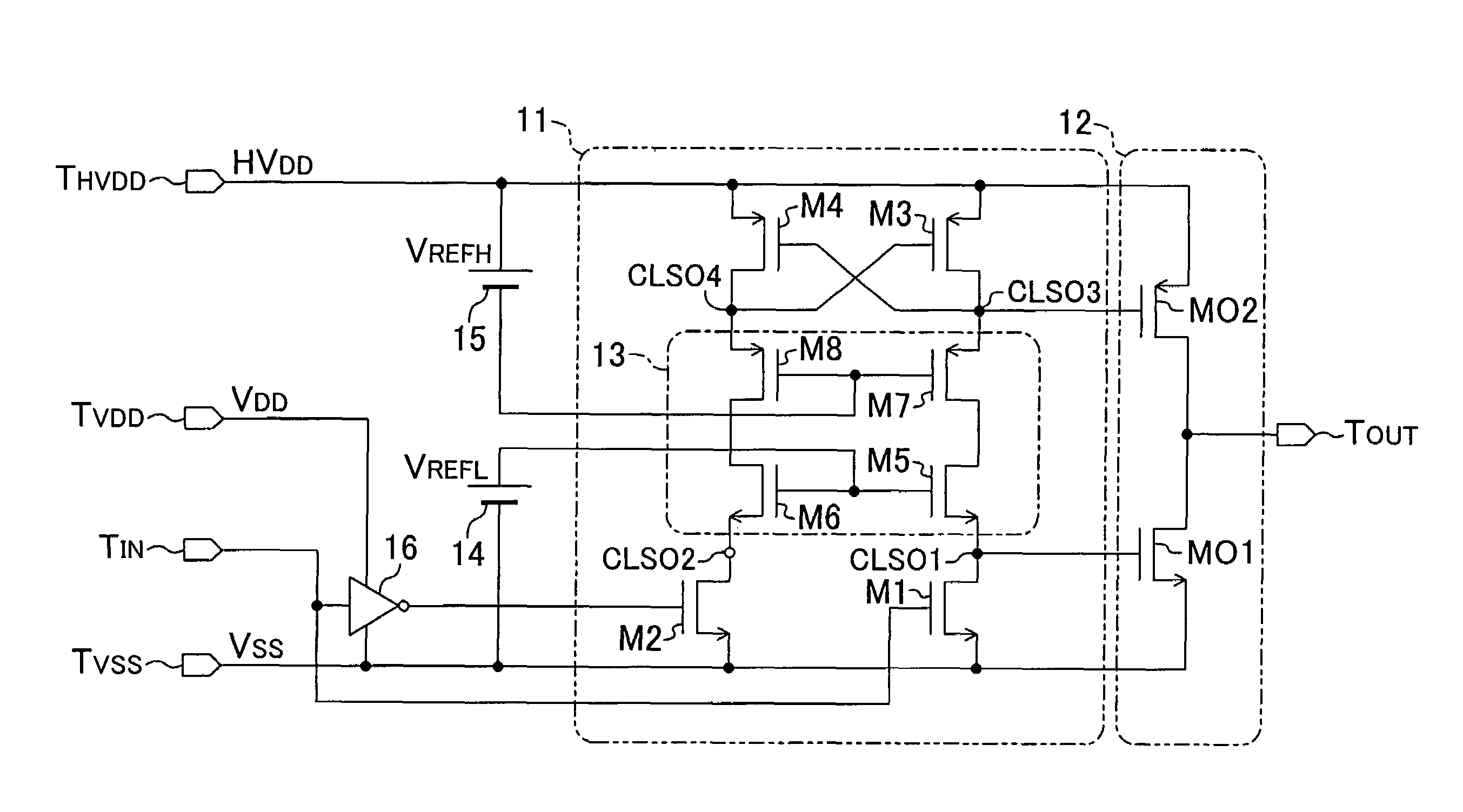
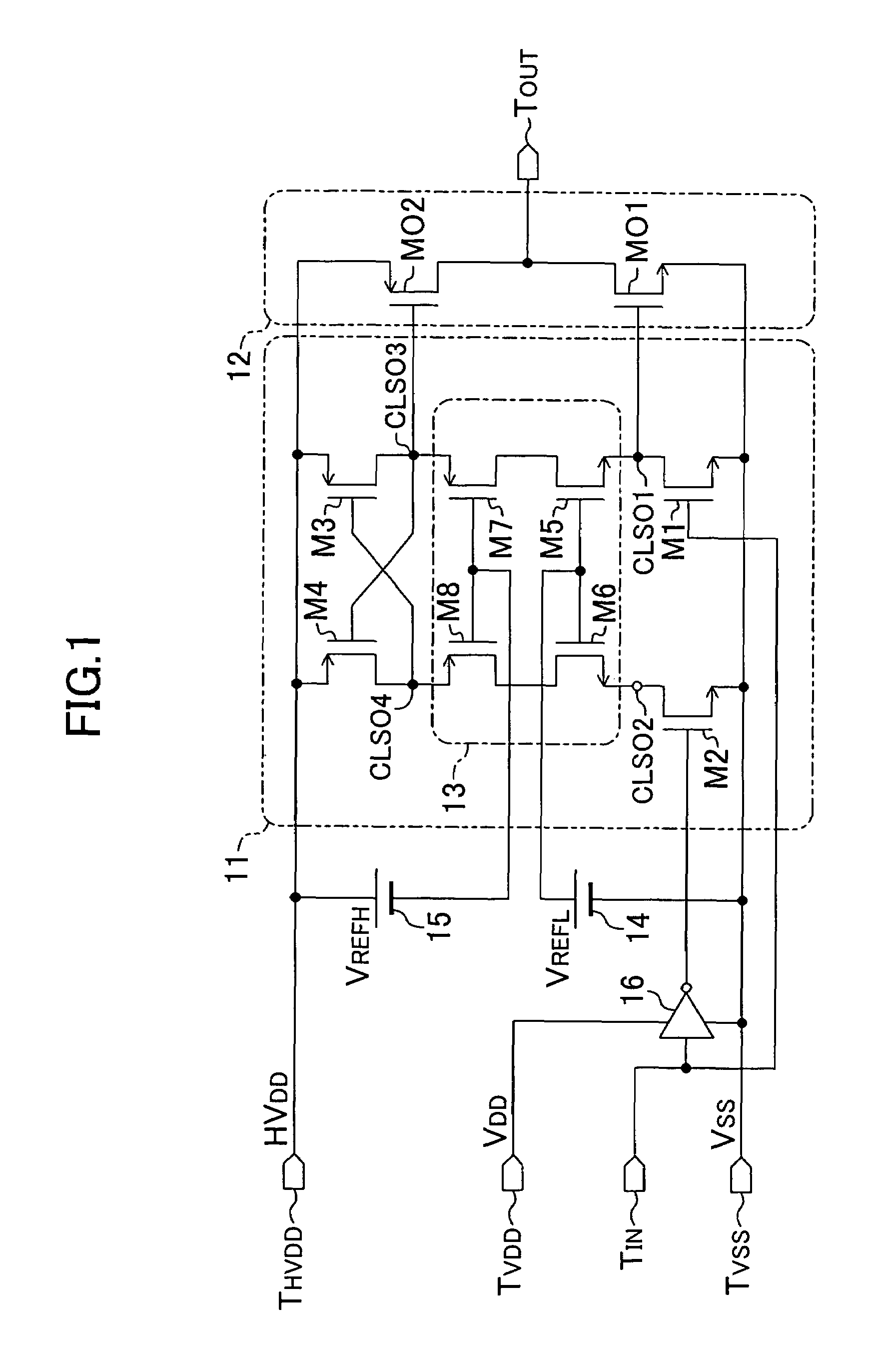
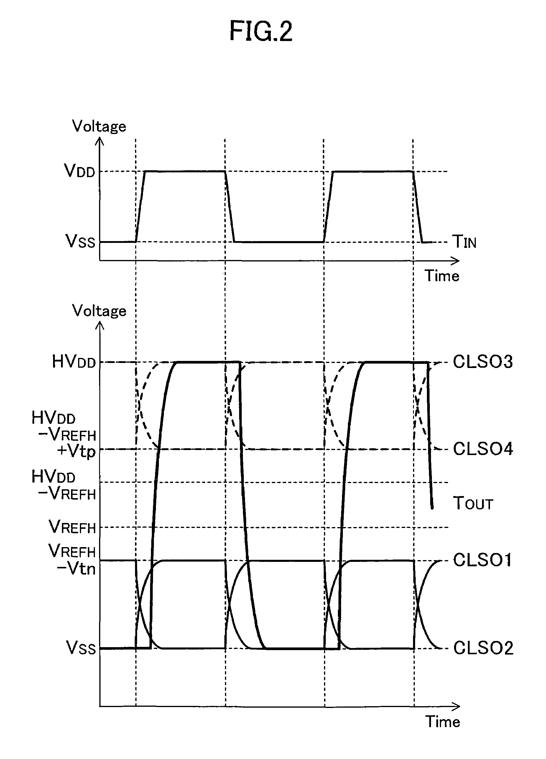
Level shift circuit

a level shift circuit and level shift technology, applied in logic circuits, pulse automatic control, pulse techniques, etc., can solve the problems of high-breakdown-voltage transistors and low-breakdown-voltage transistors in mixed relation, complex circuit design and fabrication process, and high-breakdown-voltage capacitors

Inactive Publication Date: 2008-03-25
PANASONIC CORP
View PDF3 Cites 27 Cited by
  • Summary
  • Abstract
  • Description
  • Claims
  • Application Information

AI Technical Summary

Benefits of technology

[0011]It is therefore an object of the present invention to solve the conventional problem described above and allows a level shift circuit which features easy circuit design and easy fabrication and outputs a signal with an amplitude exceeding the gate-source breakdown voltage of each of transistors composing the circuit to be implemented without using a high-breakdown-voltage capacitor.

Problems solved by technology

A circuit which includes a high-breakdown-voltage transistor and a low-breakdown-voltage transistor in mixed relation is complicated in circuit design and fabrication process.
Moreover, since the high-breakdown-voltage transistor is large in size, the area occupied by the semiconductor device is increased disadvantageously.
However, the conventional level shift circuit mentioned above has the problem that it requires a high-breakdown-voltage capacitor.
Therefore, the conventional level shift circuit need not use a transistor with a high gate-source breakdown voltage, but the effect of reducing the area occupied by the semiconductor device can hardly be expected therefrom.

Method used


Image

  • Level shift circuit
  • Level shift circuit
  • Level shift circuit

Examples


embodiment 1

Variation of Embodiment 1

[0043]A variation of the first embodiment will be described herein below with reference to the drawings. Since the level shift circuit according to the first embodiment can use a transistor having a low gate-source breakdown voltage even as the output transistor, a CMOS structure is used for each of the transistors composing the circuit. However, there is a case where a higher-voltage output is required. In such a case, the source-drain breakdown voltage presents a problem. For example, when an output of not less than 20 V is required, the source-drain breakdown voltage of a typical CMOS transistor is insufficient. In that case, a transistor having a DMOS (Double diffused MOS) structure may be used appropriately as the output transistor.

[0044]FIG. 3 shows a cross-sectional structure of a typical N-polarity DMOS transistor. A gate electrode 52 having a gate oxide film 51 is formed on an N-well 58 provided in the region of a substrate 50 isolated by the isolat...

embodiment 2

[0048]A second embodiment of the present invention will be described herein below with reference to the drawings. FIG. 4 shows a circuit structure of a level shift circuit according to the second embodiment. The description of the components shown in FIG. 4 which are the same as those shown in FIG. 1 will be omitted by retaining the same reference numerals.

[0049]In the level shift circuit according to the present embodiment, the voltage HVDD applied to the high-voltage power source terminal THVDD has a wide operation range. Even when the lower limit value of the voltage HVDD is lower than the gate-source breakdown voltage of any of the transistors composing the circuit, the level shift circuit can be driven at a high speed.

[0050]In the first embodiment, the first and second bias voltages VREFL and VREFH have been set appropriately such that each of the values (VREFL−Vtn) and (VREFH−Vtp) does not exceed the gate-source breakdown voltage of the transistor. However, the first and secon...


PUM


Abstract

A level shift circuit has a driving circuit and an output circuit. The driving circuit has a clamp circuit for receiving first and second bias potentials, outputting first and second drive signals which are not less than a reference potential, less than the first bias potential, and complementary to each other, and also outputting third and fourth drive signals which are higher than the second bias potential, not more than a power source potential, and complementary to each other. The output circuit has a first output transistor of a first conductivity type and a second output transistor of a second conductivity type which are connected in series to each other. The first output transistor has a gate for receiving the first drive signal and one electrode for receiving the reference potential. The second output transistor has a gate for receiving the third drive signal and one electrode for receiving the power source potential.

Description

CROSS REFERENCE TO RELATED APPLICATIONS[0001]The teachings of Japanese Patent Application JP 2005-304447, filed Oct. 19, 2005, are entirely incorporated herein by reference, inclusive of the claims, specification, and drawings.BACKGROUND OF THE INVENTION[0002]The present invention relates to a level shift circuit for outputting a signal with a high-voltage amplitude.[0003]In recent years, as semiconductor devices have been reduced further in size and power consumption, power source voltages have increasingly lowered. On the other hand, circuits which require high-voltage drive signals are still present so that a level shift circuit for outputting a signal with a high-voltage amplitude is in demand. In the level shift circuit, it is normally necessary to adjust the gate-source breakdown voltage of an output-stage transistor to a level higher than the amplitude voltage of an output signal therefrom. A circuit which includes a high-breakdown-voltage transistor and a low-breakdown-volta...

Claims


Application Information

Patent Timeline
Patent Type & Authority Patents(United States)
IPC IPC(8): H03K19/0175
CPCH03K3/356104
Inventor KOTO, MASAAKIKIMURA, KAZUHITOISHII, TAKUYAMORITAKE, KAZUYUKI
Owner PANASONIC CORP
Why Eureka
Try Eureka