Optical scanning module, device, and method, and imaging apparatus
a scanning module and optical technology, applied in the field of optical scanning modules, devices, and methods, can solve the problems of difficult correction limited high-speed scanning, and long service life of optical scanning devices, so as to reduce power consumption, improve effective scanning rate, and improve the effect of image recording
- Summary
- Abstract
- Description
- Claims
- Application Information
AI Technical Summary
Benefits of technology
Problems solved by technology
Method used
Image

Examples
first embodiment
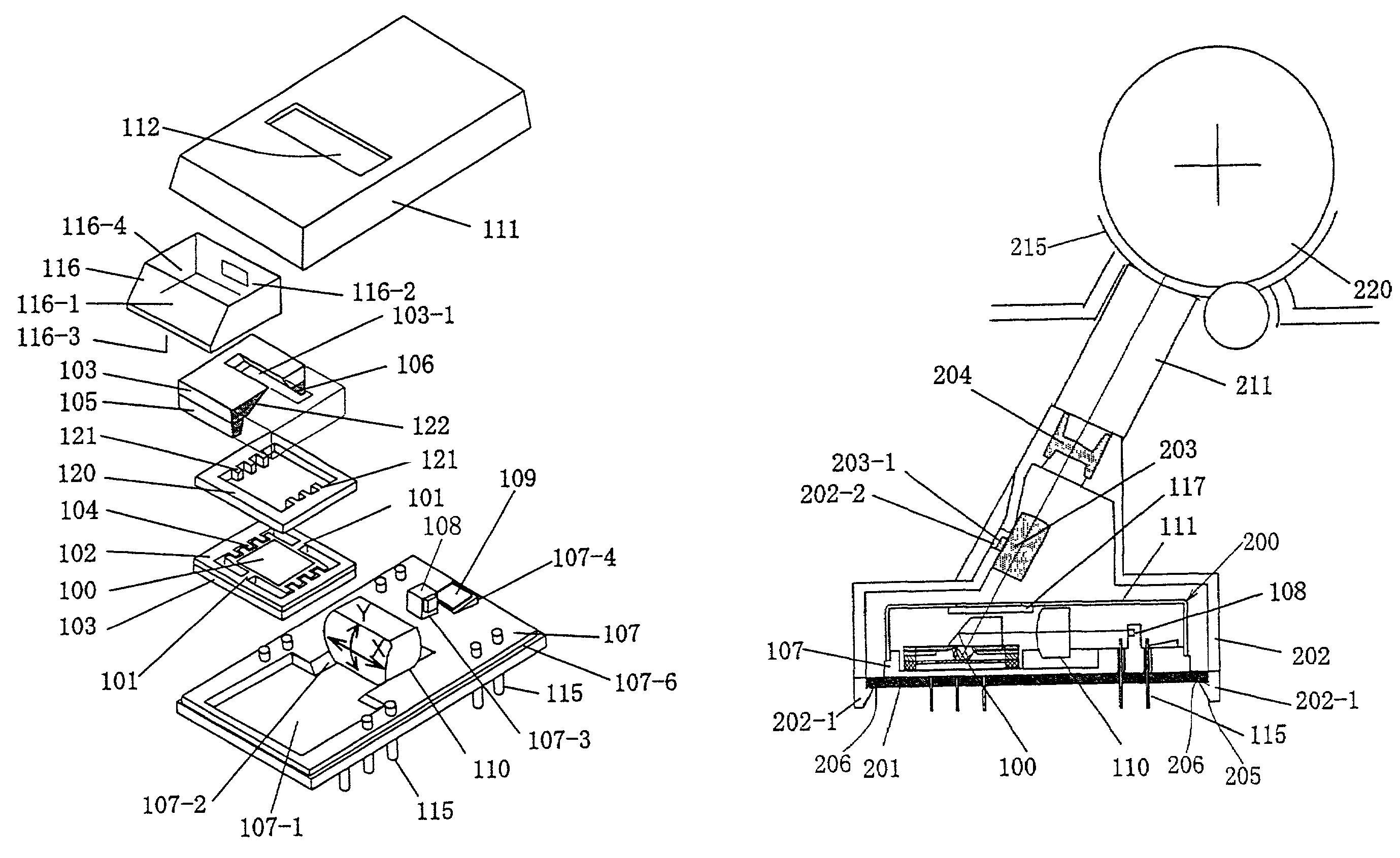
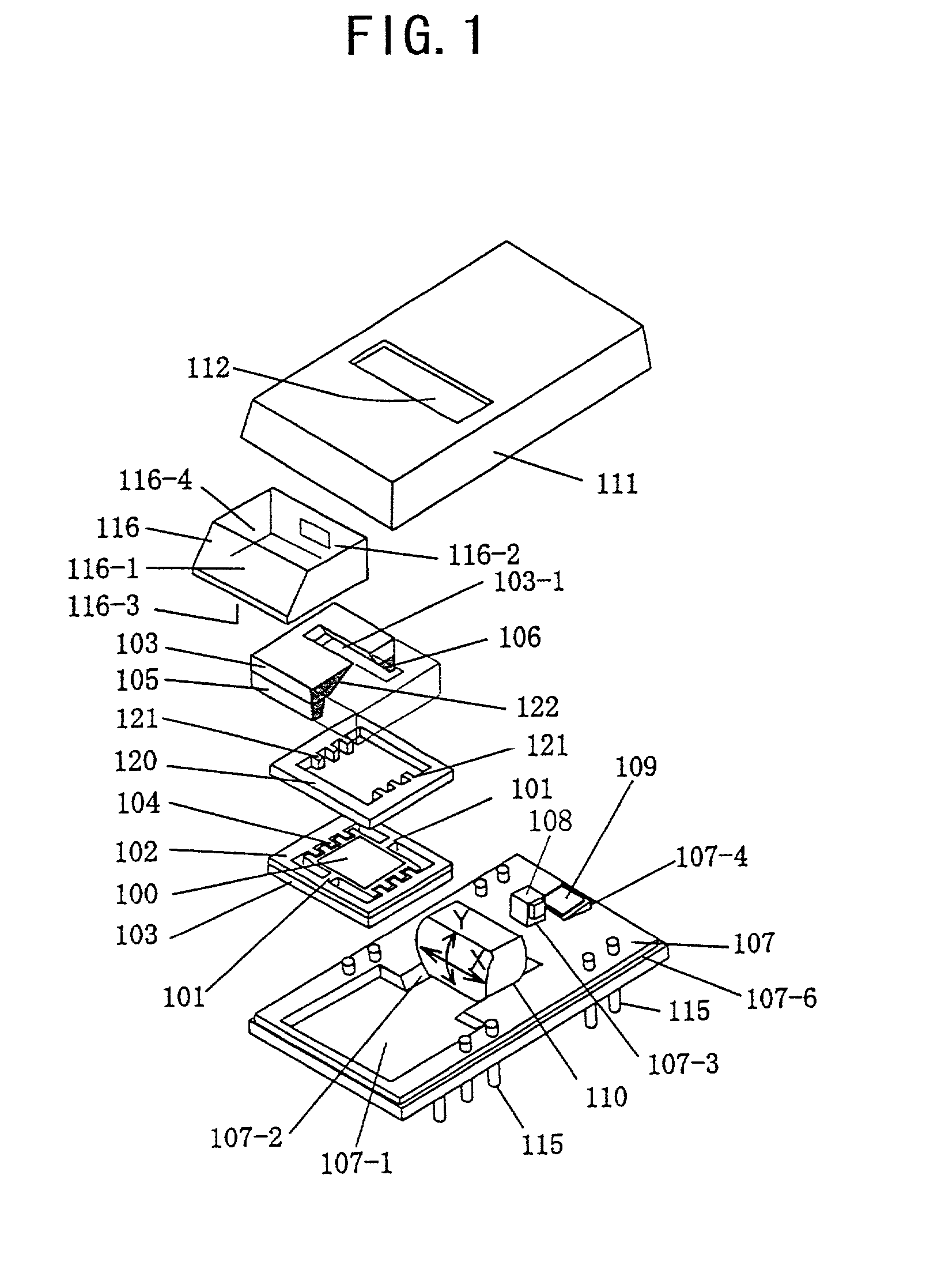
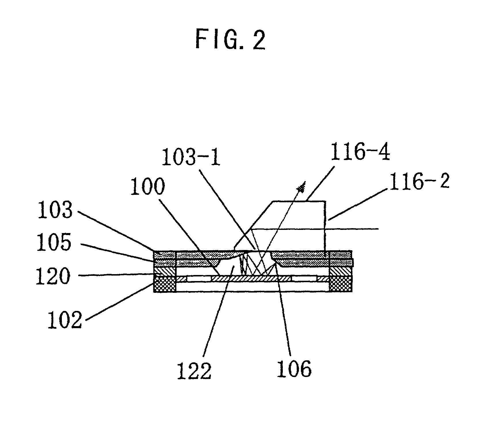
[0069]FIG. 1 is an exploded perspective view of an optical scanning module provided in an optical scanning device according to the present invention. In FIG. 1, a mirror substrate 102 is formed by first forming a square hole in the bottom of a silicon substrate by etching so that a frame part of a given thickness and a top plate part of a given thickness are formed in the silicon substrate and then forming through holes in the top plate part so that a movable mirror 100 and torsion bars 101 turnably supporting the movable mirror 100 are formed therein, surrounded by the through holes.
[0070]The movable mirror 100 has a mirror surface formed of a vapor-deposited metal film in its center part. Side edge parts of the movable mirror 100 extending along the torsion bars 101 are formed of convex and concave parts arranged like comb teeth, and form movable electrodes 104. The movable mirror 100 oscillates in a hollow part or the square hole formed in the bottom of the mirror substrate 102. ...
second embodiment
[0081]FIG. 3 is a sectional view of an optical scanning device according to the present invention. FIGS. 4A and 4B are perspective views of the optical scanning device of FIG. 3. First through third optical scanning modules 200a through 200c according to the above-described configuration are arranged in the primary scanning direction on a printed board 201 on which electronic components forming the driving circuits of the LDs and the movable mirrors 100 of the optical scanning modules 200a through 200c are mounted. In mounting the optical scanning modules 200a through 200c on the printed board 201, each of the support frames 107 has its bottom surface contacting the printed board 201 with the lead terminals 115 protruding downward from its bottom surface being inserted into corresponding through holes formed in the printed board 201. Then, the optical scanning modules 200a through 200c are positioned on the printed board 201 with respect to each other within the clearances of the th...
third embodiment
[0087]FIG. 5 is a sectional view of a color laser printer according to the present invention to which printer the optical scanning devices of the present invention are applied.
[0088]An optical scanning device 520 according to the above-described configuration and a process cartridge 500 are positioned for each of colors (yellow, magenta, cyan, and black) and provided in series in a paper-conveying direction indicated by arrow in FIG. 5 in the color laser printer. A paper sheet is supplied from a paper feed tray 506 by a paper feed roller 507, and fed in timing with printing by a registration roller 508. Then, the paper sheet is conveyed in the paper-conveying direction on a conveyer belt 511. A toner image of each color formed by an electrostatic attraction is transferred to the paper sheet when the paper sheet passes each photosensitive body drum (an image holding body) 501 so that the color images are successively superimposed one over the other to be fixed on the paper sheet by a...
PUM
 Abstract
Description
Claims
Application Information
 - R&D Engineer
- R&D Manager
- IP Professional
- Industry Leading Data Capabilities
- Powerful AI technology
- Patent DNA Extraction
Browse by: Latest US Patents, China's latest patents, Technical Efficacy Thesaurus, Application Domain, Technology Topic.
© 2024 PatSnap. All rights reserved.Legal|Privacy policy|Modern Slavery Act Transparency Statement|Sitemap