

Techniques for providing calibrated parallel on-chip termination impedance
a technology of termination resistor and parallel impedance, which is applied in the field of electromechanical circuits, can solve the problems of large number of termination resistors and degrading signal integrity
- Summary
- Abstract
- Description
- Claims
- Application Information
AI Technical Summary
Benefits of technology
Problems solved by technology
Method used
Image

Examples
Embodiment Construction
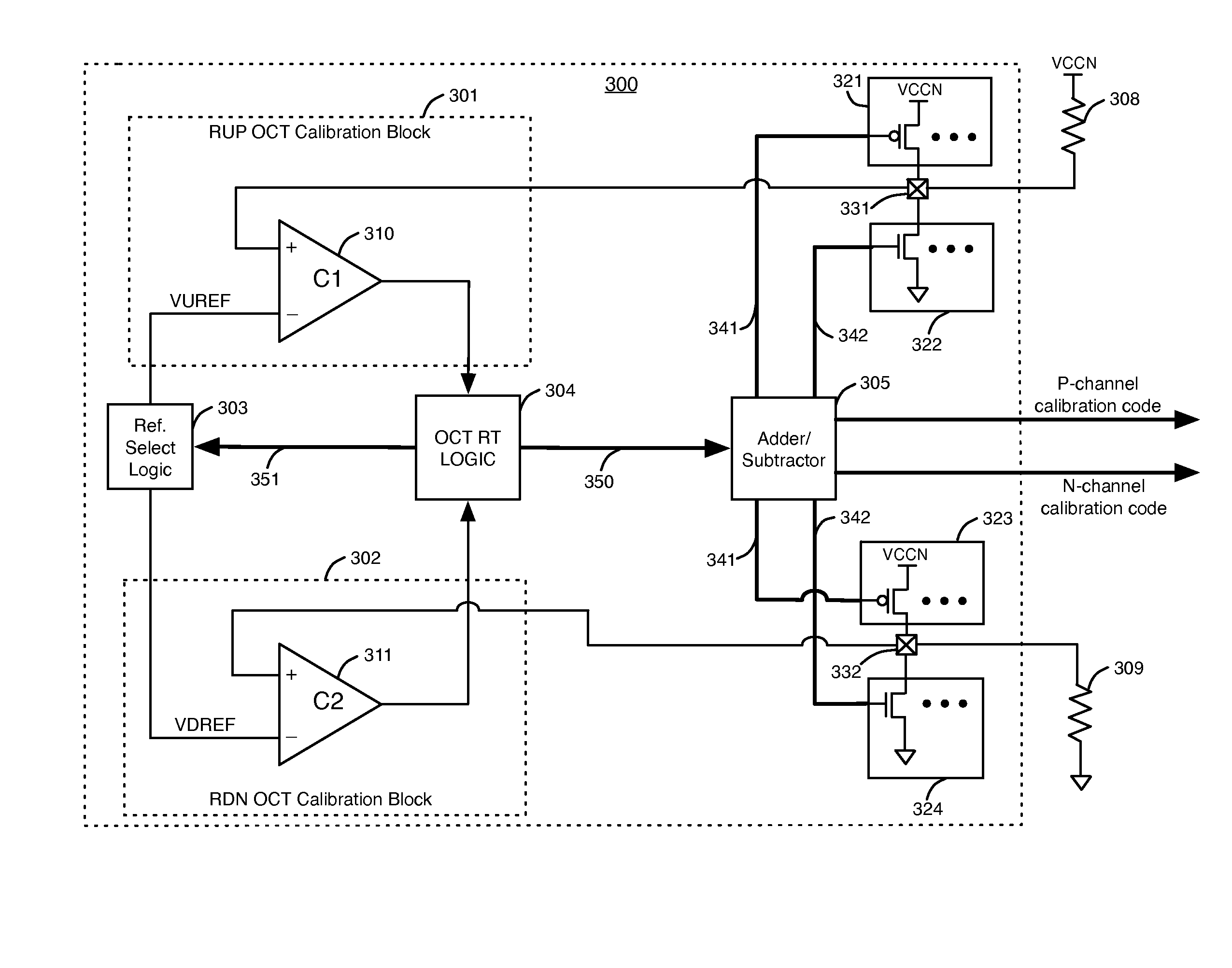
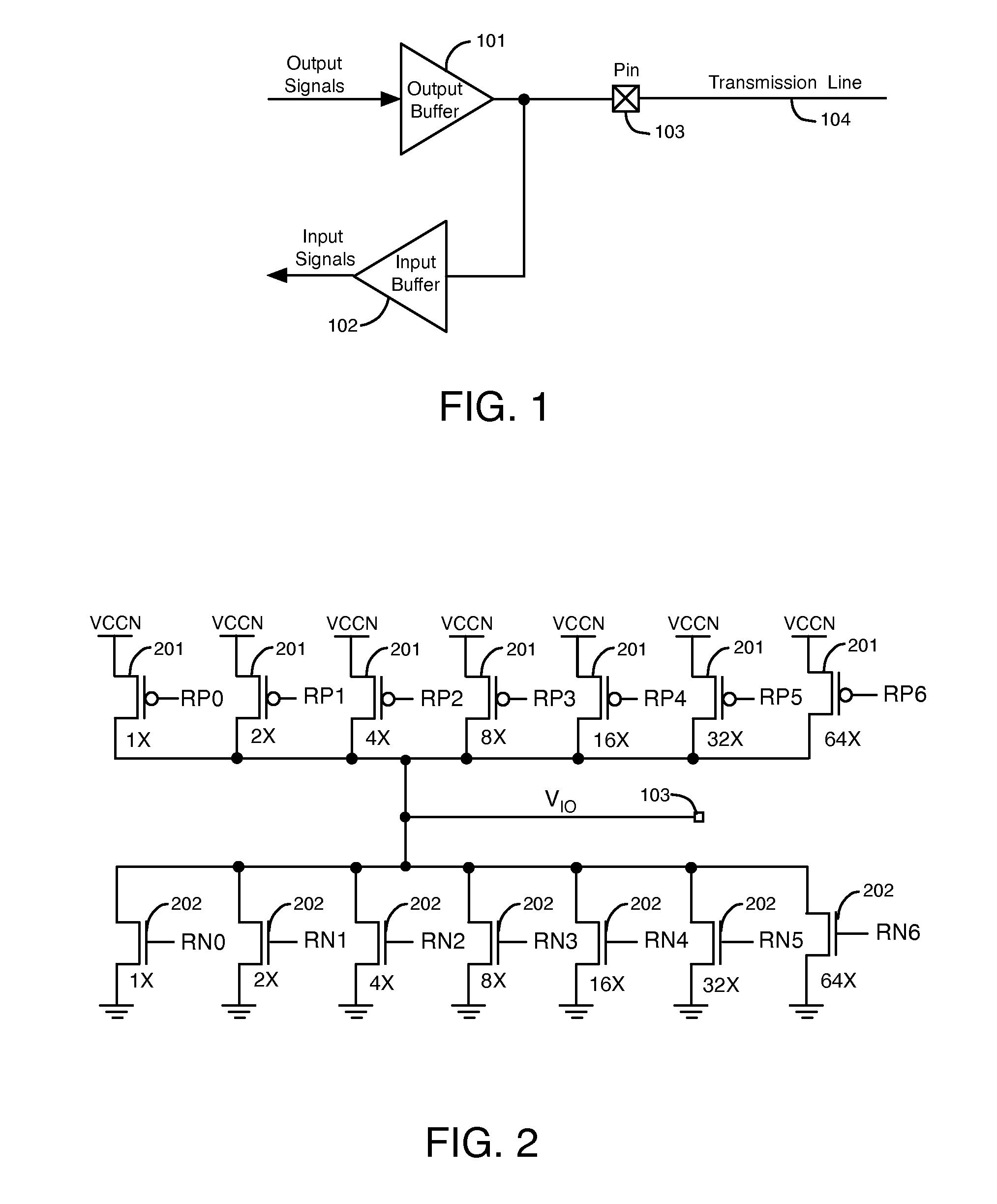
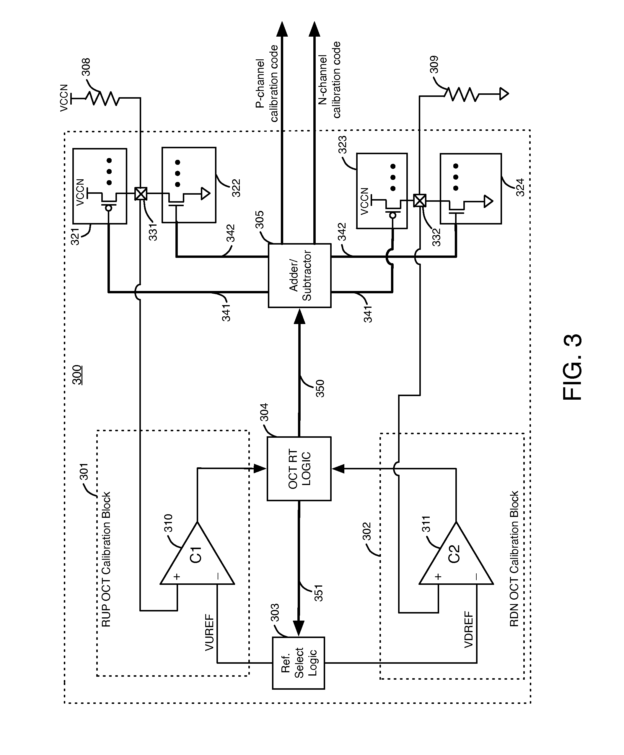
[0018]FIG. 1 illustrates an output buffer 101 and an input buffer 102 that are coupled to a pin 103 on an integrated circuit, according to an embodiment of the present invention. A transmission line 104 is coupled to pin 103. Output buffer 101 drives output signals to transmission line 104 through pin 103. Output buffer 101 contains P-channel and N-channel transistors that drive the output signals to transmission line 104. Examples of these transistors are shown in FIG. 2.
[0019]FIG. 2 illustrates 7 P-channel MOS field-effect transistors 201 that are coupled together in parallel, and 7 N-channel MOS field-effect transistors 202 that are coupled together in parallel in output buffer 101, according to an embodiment of the present invention. Transistors 201-202 have binary weighted width-to-length (W / L) channel ratios (e.g., 2×, 2×, 4×, 8×, 16×, 32×, 64×) as shown in FIG. 2. The drains of transistors 201 and 202 are coupled to pin 103. The voltage at pin 103 is VIO.
[0020]Transistors 201...
PUM
 Abstract
Description
Claims
Application Information