Controlling operation of flash memories

a technology for controlling the operation of flash memory and memory devices, applied in the direction of instruments, computing, electric digital data processing, etc., can solve the problems of adversely affecting the read/write throughput, the possibility of ascertaining, and the inability to ascertain

Active Publication Date: 2008-11-25
MICRON TECH INC
View PDF16 Cites 27 Cited by
  • Summary
  • Abstract
  • Description
  • Claims
  • Application Information

AI Technical Summary

Problems solved by technology

In fact, if the cell B absorbs current (1), it is not possible to ascertain whether the cell A is absorbing current (1) or not (0).
In fact, if the cell B does not absorb any current (0), it is not possible to ascertain whether the cell A is absorbing current (1) or not (0) because otherwise the circuit would be interrupted.
Therefore, read / write throughput is adversely affected by these additional operations.

Method used


Image

  • Controlling operation of flash memories
  • Controlling operation of flash memories
  • Controlling operation of flash memories

Examples


Embodiment Construction

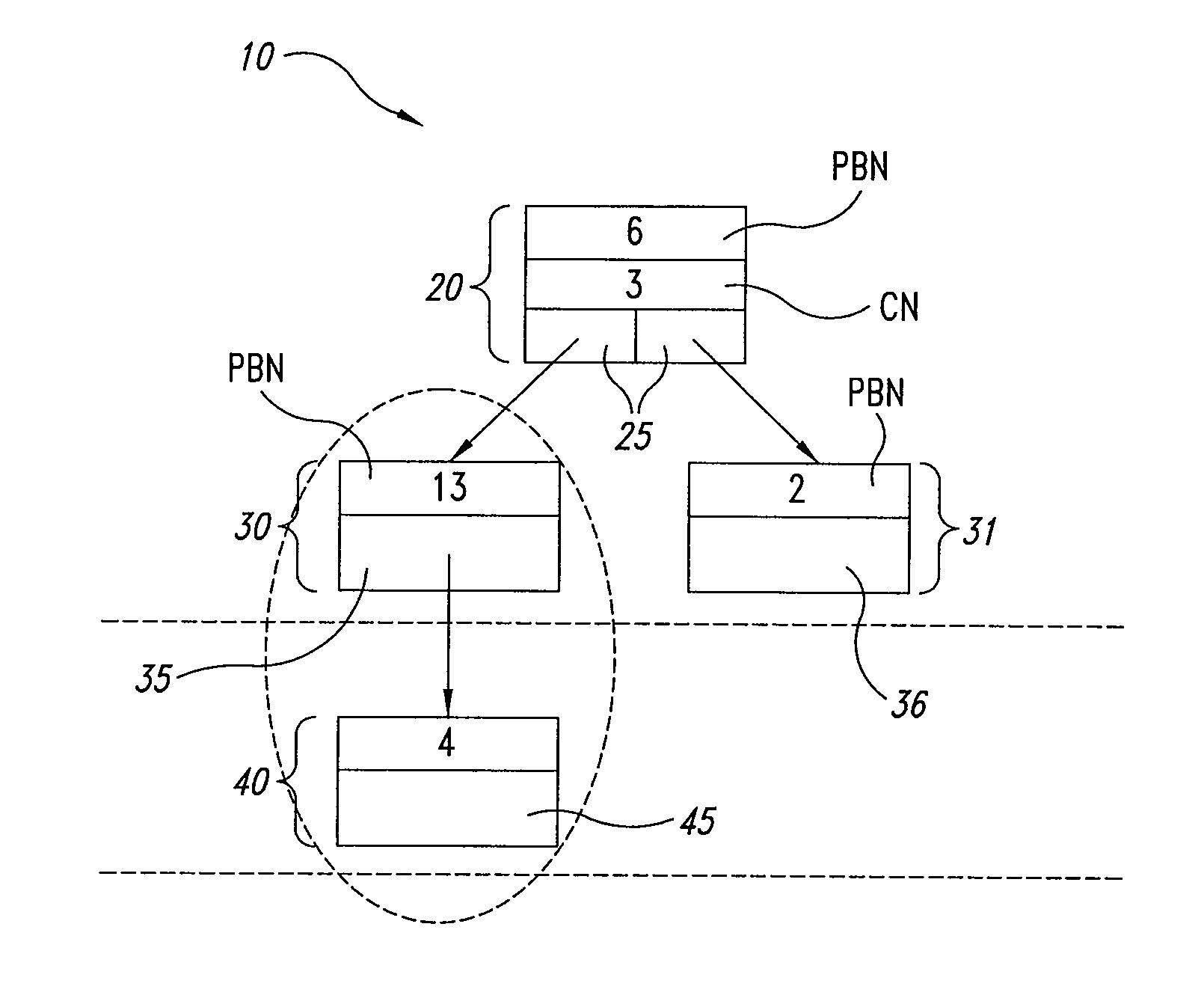
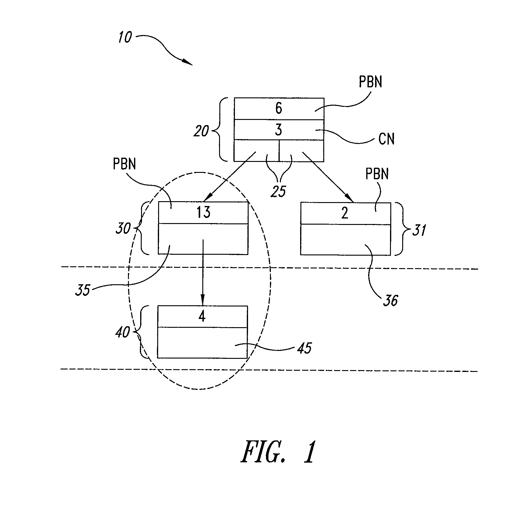
[0037]The solution described herein is based on the use of a virtual-to-physical mapping table. The virtual-to-physical mapping table stores, for each entry, a pointer to a tree structure instead of a physical block number. Each tree structure links logically a set of physical blocks in the flash device. All the physical blocks indicated in the tree data structure refer to the same virtual block.

[0038]The solution described-herein stores information used to link the blocks that are part of the tree data structure. Such information is stored in spare area of the first page of each block of the tree.

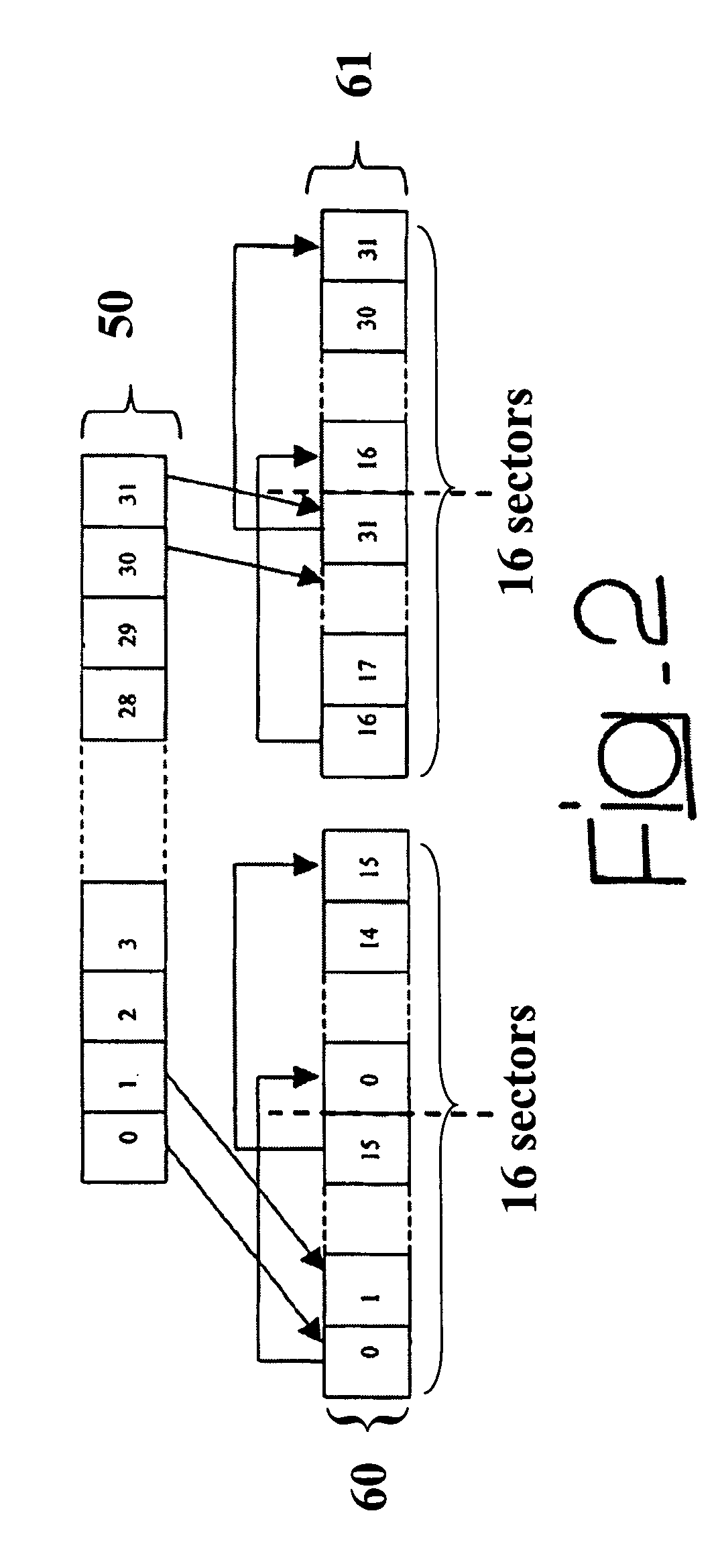
[0039]Additionally, the solution permits to write updates of a page in a different position of the same physical block. In particular, the solution writes the new version of a page in a defined position that can be calculated starting from page position in a virtual block. Therefore no need exists of reading the spare area of any pages to learn the new position of a page.

[0040]This feature...


PUM


Abstract

A method controls write / erase operations in a memory device, such as a NAND flash memory. The method includes dividing the memory device in physical blocks, wherein each physical block is comprised of a number of pages; considering the memory device as comprising consecutive virtual blocks, each virtual block including consecutive sectors; associating to each virtual block a virtual block number; selecting the size of the virtual blocks equal to a multiple of the size of the physical blocks; and creating a virtual-to-physical mapping table having entries. Each entry in the mapping table stores a pointer to a root node of a tree structure that links logically a set of physical blocks in the memory device.

Description

BACKGROUND OF THE INVENTION[0001]1. Field of the Invention[0002]The invention relates to techniques for controlling operation of memory devices, and was developed by paying specific attention to the possible application in NAND flash memories that store information in NAND cells.[0003]2. Description of the Related Art[0004]In embedded operating systems, file systems read and write data in small blocks of a hard disk called “sectors”, typically of the size of 512 bytes.[0005]In some embedded systems, rather than in the hard disk, the data are saved in NAND flash memories.[0006]The designation “NAND” derives form the specific matrix-like organization (specifically related to the bit lines) of connecting the floating gate cells of the same string (typically 11 or 32) in series (between a drain switch—connected to the bit line—and a source switch). This implies a specific truth table for reading. In fact for reading a given cell in the string (the other strings being de-selected by the ...

Claims


Application Information

Patent Timeline
Patent Type & Authority Patents(United States)
IPC IPC(8): G06F12/00
CPCG06F12/0246
Inventor DI SENA, ANGELOINTINI, AGATA
Owner MICRON TECH INC
Why Eureka
Try Eureka