
Mask, method for forming a pattern, and method for evaluating pattern line width

a mask and pattern technology, applied in the field of masks, can solve problems such as the determination of the line width of mask patterns, and achieve the effect of masks, and reducing the number of masks

Inactive Publication Date: 2008-12-02
FUJITSU SEMICON LTD
View PDF5 Cites 0 Cited by
  • Summary
  • Abstract
  • Description
  • Claims
  • Application Information

AI Technical Summary

Benefits of technology

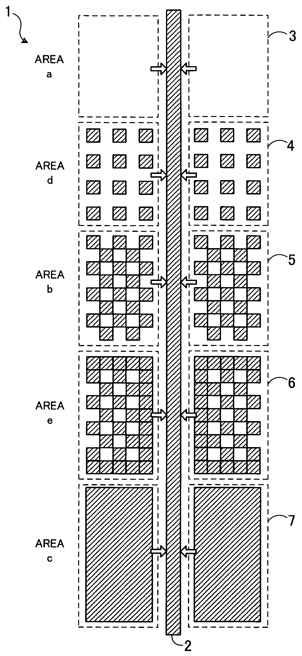
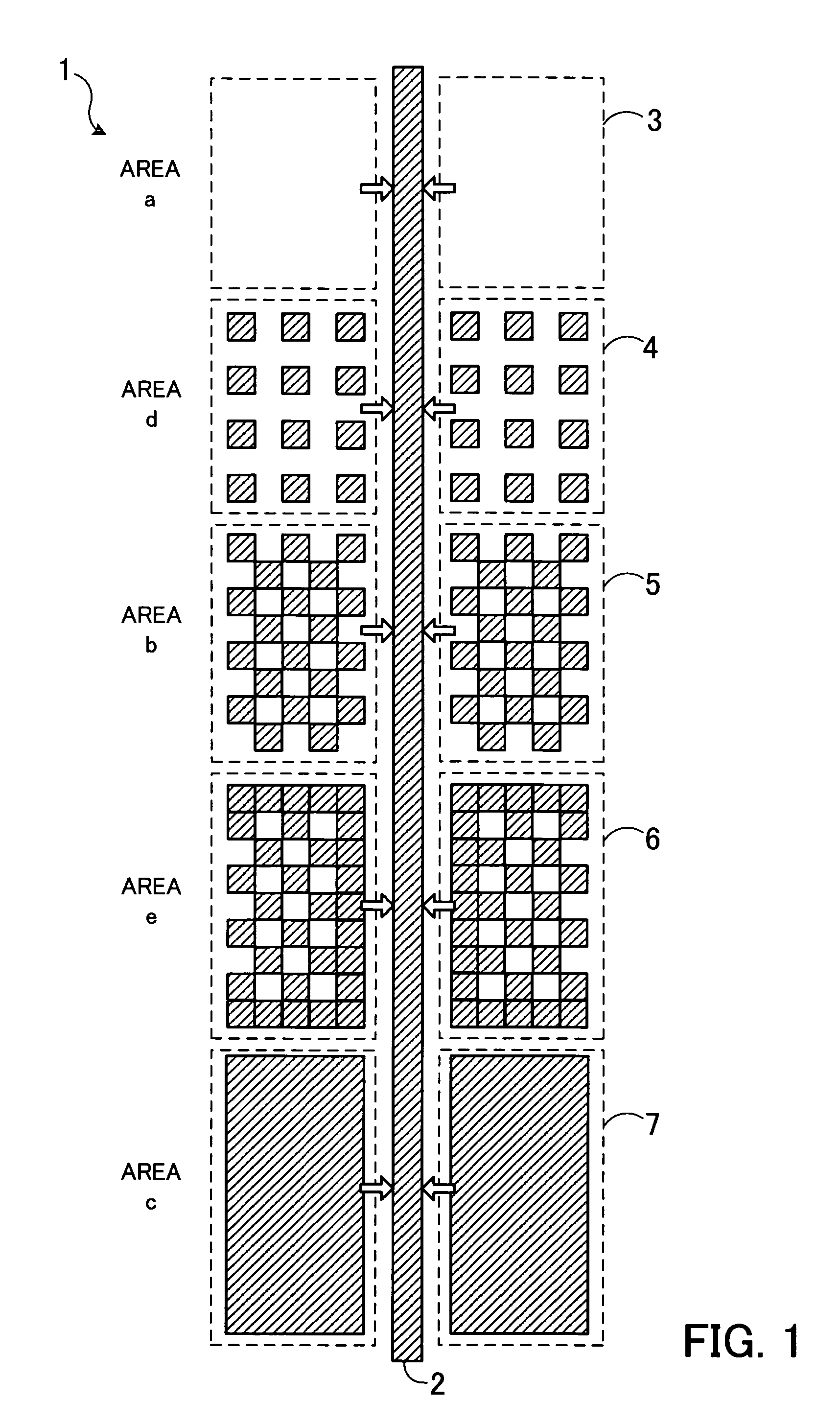
"The present invention provides a mask with a mask pattern that includes a pattern to be determined and multiple surrounding patterns. The mask pattern is designed such that the pattern to be determined is located between a pair of surrounding patterns with a same aperture rate. The method for forming the pattern includes forming the pattern to be determined and then forming a pair of surrounding patterns with a same aperture rate near the pattern. The pattern line width evaluation method includes forming multiple pairs of surrounding patterns with a same aperture rate, determining the line width of the pattern to be determined in each area between the pairs of surrounding patterns, and using the line width of one area as a standard to compare with the line width of another area and find the amount of determination error caused by charge-up. The technical effects of this invention include improving pattern accuracy and reducing charge-up effects."

Problems solved by technology

In many cases, this causes an error in the line width of the mask pattern determined on the basis of the SEM image.

Method used


Image

  • Mask, method for forming a pattern, and method for evaluating pattern line width
  • Mask, method for forming a pattern, and method for evaluating pattern line width
  • Mask, method for forming a pattern, and method for evaluating pattern line width

Examples


Embodiment Construction

[0024]Conventionally, whether charge-up influences a result obtained by determining the line width of a mask pattern formed on a photo mask has not been considered. Furthermore, the amount of a determination error caused by charge-up has conventionally not been found quantitively. Accordingly, even if charge-up has an influence on the determination of the line width, it is impossible to recognize the extent of the influence. Therefore, when the line width of a mask pattern is evaluated, the line width may or may not be determined accurately. It is difficult to judge whether the line width of the pattern is evaluated properly.

[0025]The present invention was made to solve such a problem. An object of the present invention is to provide a mask having a mask pattern for properly evaluating the line width of a pattern and a method for forming such a pattern.

[0026]Another object of the present invention is to provide a pattern line width evaluation method for properly evaluating the line ...


PUM

PropertyMeasurementUnit
thicknessaaaaaaaaaa
thicknessaaaaaaaaaa
thicknessaaaaaaaaaa

Abstract

A mask having a mask pattern for properly evaluating pattern line width. A mask pattern including a pattern to be determined and a plurality of surrounding patterns is formed on a mask. Areas with the same line width in the pattern to be determined are located between a pair of surrounding patterns with an aperture rate of 0%, between a pair of surrounding patterns with an aperture rate of 50%, and between a pair of surrounding patterns with an aperture rate of 100%, respectively. These pairs of surrounding patterns with the different aperture rates change the influence of charge-up on the pattern to be determined. Accordingly, the line width of each area in the pattern to be determined is determined, the difference between the line width of two areas is found, and the amount of a determination error caused by the charge-up is calculated. As a result, whether the line width of the pattern is determined with accuracy can be judged and the line width of the pattern can be evaluated properly.

Description

CROSS-REFERENCE TO RELATED APPLICATIONS[0001]This application is based upon and claims the benefits of priority from the prior Japanese Patent Application No. 2004-204052, filed on Jul. 12, 2004, the entire contents of which are incorporated herein by reference.BACKGROUND OF THE INVENTION[0002](1) Field of the Invention[0003]This invention relates to a mask, a method for forming a pattern, and a method for evaluating the line width of a pattern and, more particularly, to a mask used for evaluating the line width of a mask pattern formed on a photo mask, a method for forming such a pattern, and a method for evaluating the line width of such a pattern.[0004](2) Description of the Related Art[0005]Control of the line width, such as the gate line width, of circuit patterns in semiconductor devices is very important in fabricating them. To form a circuit pattern, a photo mask where a mask pattern which is usually four or five times the size of the circuit pattern is formed is used. This ...

Claims


Application Information

Patent Timeline
Patent Type & Authority Patents(United States)
IPC IPC(8): G03F1/00G03C5/02G03F1/44G03F1/70H01L21/027
CPCG03F1/14G03F1/44
Inventor YAMAUCHI, SATOSHI
Owner FUJITSU SEMICON LTD
Learn More