Method for preventing a metal corrosion in a semiconductor device

a technology of semiconductor devices and metal layers, which is applied in the direction of semiconductor/solid-state device manufacturing, basic electric elements, electric devices, etc., can solve the problems of not preventing the corrosion of aluminum wirings, the effect of reducing the yield of manufacturing semiconductor devices, and little effect on the removal of chlorine residues, so as to improve the profile of metal layers and prevent metal corrosion. , the effect of improving the reliability and yield of semiconductor devices

Inactive Publication Date: 2008-12-23
DONGBU ELECTRONICS CO LTD
View PDF10 Cites 175 Cited by
  • Summary
  • Abstract
  • Description
  • Claims
  • Application Information

AI Technical Summary

Benefits of technology

[0014]It is, therefore, an object of the present invention to provide a method for preventing metal corrosion in a semiconductor device (and, in one embodiment, simultaneously preventing formation of a bridge between metal wirings), thereby improving the profile of metal layer and the reliability and yield of the semiconductor device.

Problems solved by technology

The corrosion defects 112 deteriorate the electrical performance of the semiconductor device or integrated circuit, or cause failures such as a short circuit thus decreasing the yield of manufacturing the semiconductor device.
However, the first method has little effect on removal of the chlorine residues, and generally does not prevent the corrosion of aluminum wirings in the long run.
The second method may produce or result in problems such as hillock formation, segregation, or recrystallization, etc. when the temperature of the heat treatment is over 300° C., which are generally related to the low melting point of aluminum.
However, this method may result in a problem where undercuts 114 on a titanium-containing layer (e.g., a TiN or TiW barrier) occur due to the fluorine-containing plasma, as shown in FIG. 1c.
In addition, an underlying oxide layer may be damaged, and the aluminum may be changed to AlF3 (which can result in metal degradation).
As a result, the reliability of semiconductor device may be conspicuously deteriorated.
However, there are the same problems as the above-explained method has, which are caused by plasma containing fluorine.
Moreover, these methods tend to have little effect on the prevention of corrosion.

Method used


Image

  • Method for preventing a metal corrosion in a semiconductor device
  • Method for preventing a metal corrosion in a semiconductor device
  • Method for preventing a metal corrosion in a semiconductor device

Examples


Embodiment Construction

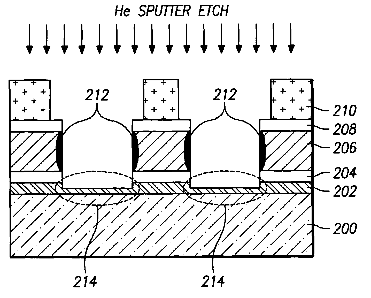
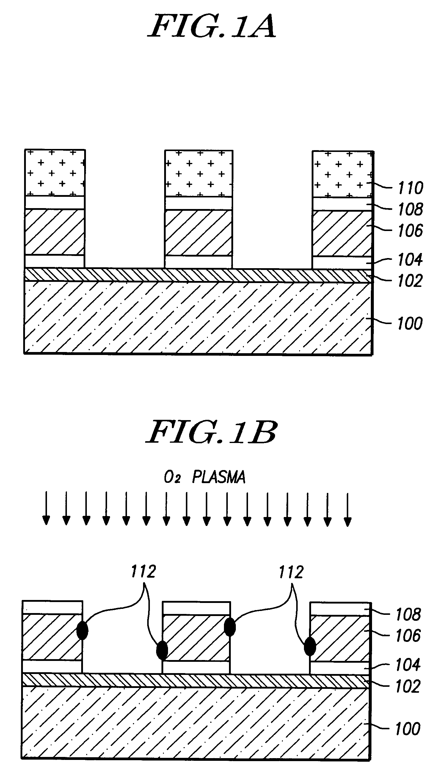
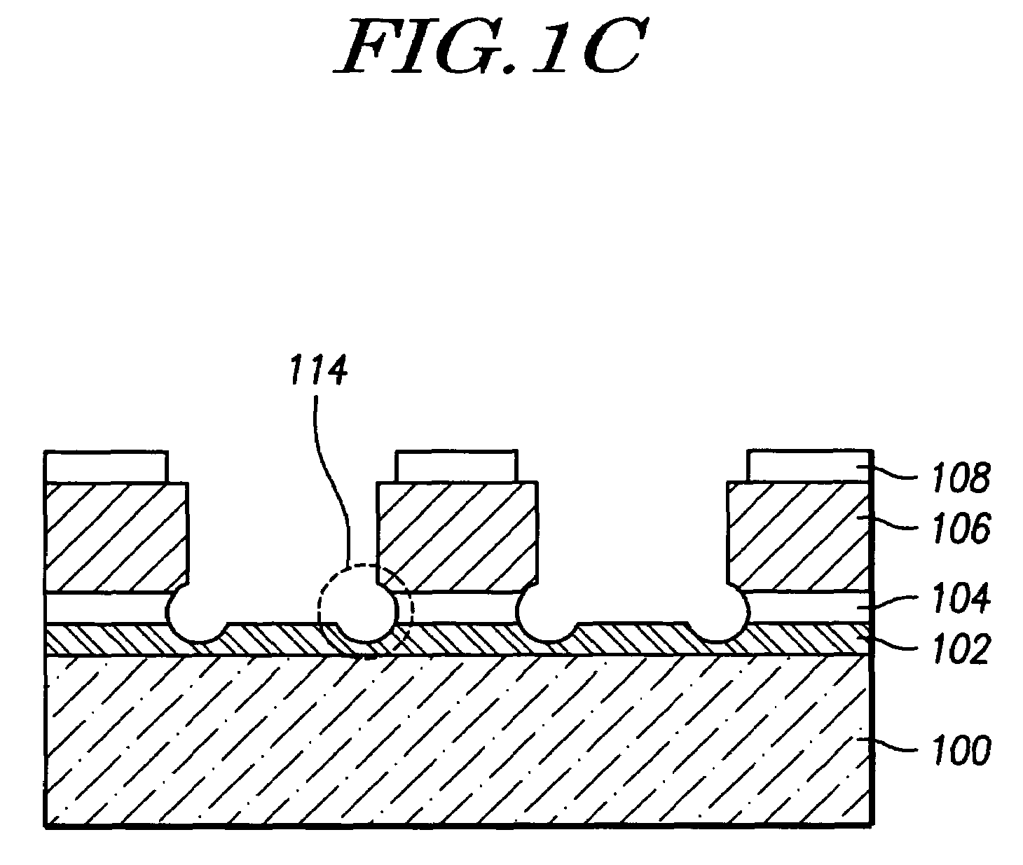
[0022]FIGS. 2a to 2d are cross-sectional views of a semiconductor device illustrating a method for preventing a metal corrosion according to the present invention.

[0023]First, as shown in FIG. 2a, a photoresist 210 is coated and patterned over a substrate 200 on which an oxide layer 202, barrier 204, metal layer 206 and antireflective coating 208 are formed in successive order. Then, antireflective coating 208, metal layer 206 and barrier 204 are dry-etched using a plasma including a chlorine source gas such as Cl2, BCl3 and / or the like. Such dry etching preferably comprises Reactive Ion Etching (RIE).

[0024]Metal layer 206 may comprise a single layer or a plurality of layers, at least one of which preferably consists essentially of aluminum, aluminum alloy (for example, Al—Cu or Al—Ti), aluminum-silicon alloy (for example, Al—Si, Al—Si—Cu, or Al—Ti—Si), and so on. However, materials are not limited to these metals or alloys thereof, and any metal or alloy thereof is available for th...


PUM

PropertyMeasurementUnit
temperatureaaaaaaaaaa
melting pointaaaaaaaaaa
pressureaaaaaaaaaa

Abstract

The present invention relates to a method for preventing a metal corrosion in a semiconductor device. The present method includes the steps of etching of a metal layer in a chamber, the metal layer having a photoresist pattern thereon or thereover; oxidizing a surface of the metal layer using a plasma comprising N2O in the same chamber; and removing the photoresist. Therefore, metal corrosion as well as bridges between metal wirings can be suppressed or prevented, thereby improving the profile of metal layer and the reliability and yield of the semiconductor device.

Description

BACKGROUND OF THE INVENTION[0001]1. Field of the Invention[0002]The present invention relates to semiconductor device manufacturing technology. More specifically, the present invention relates to a method for preventing corrosion of a metal layer in a semiconductor device, thereby enabling improvement of the reliability and yield of a semiconductor device.[0003]2. Description of the Related Art[0004]Following the rapid progress of information and communication media such as a computer, the technology of manufacturing a semiconductor device has been rapidly developed. A semiconductor device has been developed toward higher integration, miniaturization, and higher operational speed.[0005]Currently, aluminum or aluminum alloys are widely used as a wiring material for integrated circuits such as VLSI (Very Large-Scale Integration) devices, because of their superior electric conductivity and low prices. Processes of forming aluminum wiring generally comprise the steps of: forming an alum...

Claims


Application Information

Patent Timeline
Patent Type & Authority Patents(United States)
IPC IPC(8): H01L21/44
CPCH01L21/02071H01L21/31138H01L21/32136H01L21/76888H01L21/02614H01L21/0274H01L21/3065H01L21/02145
Inventor LEE, JAE SUK
Owner DONGBU ELECTRONICS CO LTD
Why Eureka
Try Eureka