Liquid crystal display device without bad pixel and method for removing bad pixel therefrom

a liquid crystal display and pixel technology, applied in the field of addressing bad (defective) pixels of the liquid crystal display device, can solve the problems of wasteful discarding of the lcd device, inferior or defective pixels formed on the corresponding lines, and inferior corresponding pixels

Inactive Publication Date: 2009-02-03
LG DISPLAY CO LTD
View PDF2 Cites 2 Cited by
  • Summary
  • Abstract
  • Description
  • Claims
  • Application Information

AI Technical Summary

Benefits of technology

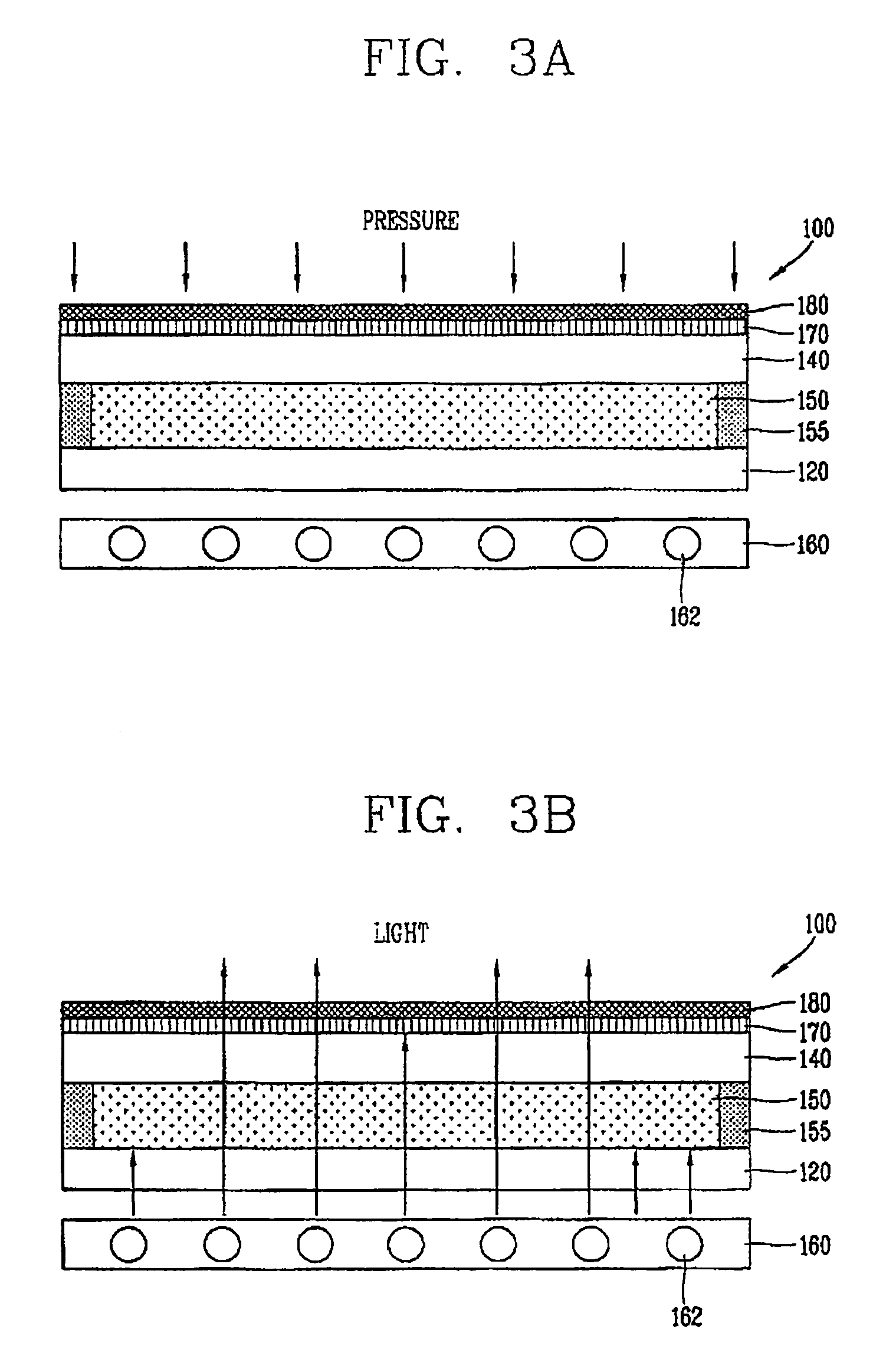
[0012]Therefore, an object of the present invention is to provide a method for removing bad (inferior) pixels of a liquid crystal display (LCD) device which is capable of preventing a user from recognizing bad pixels simply by changing a bright point of a bad pixel into a black point by preventing light from being transmitted through the bad pixel, and to provide an LCD device without bad pixels.
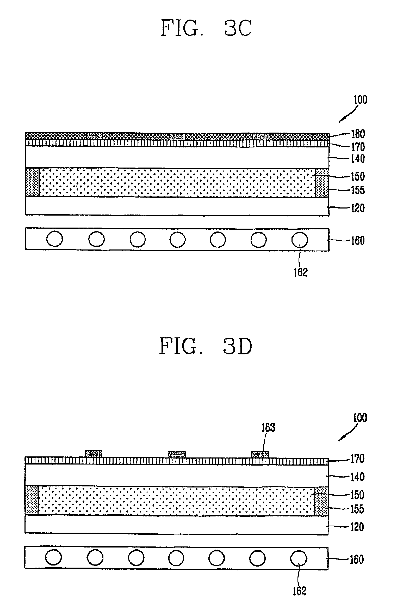
[0013]Another object of the present invention is to provide a method for removing bad pixels which is capable of removing bad pixels in a fast and inexpensive manner, wherein a black resin film is attached onto an LCD panel and the portion of the black resin film is hardened by light transmitted through a bad pixel so as to form a light shielding layer for the bad pixel, and to provide an LCD device without bad pixels.
[0014]Another object of the present invention is to provide an LCD device and a method of addressing defective pixels of the LCD device, by covering the defective pixels so as to minimize the effect of the defective pixels.

Problems solved by technology

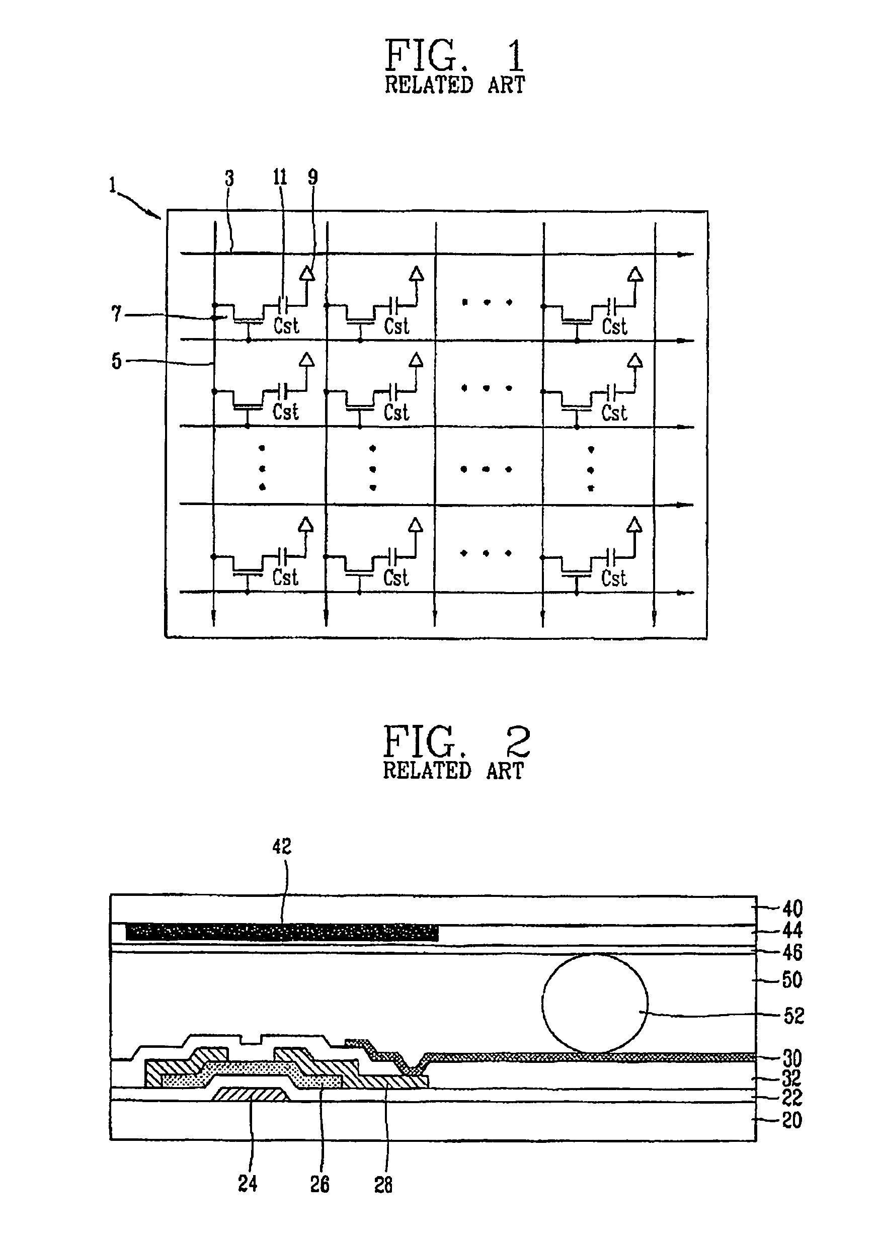
If a gate line or data line is inferior, pixels formed on the corresponding line become inferior or defective.
Also, if a TFT formed on a pixel is inferior, the corresponding pixel also become inferior.
However, it is wasteful to discard the LCD device in case that the small number of pixels are inferior.

Method used


Image

  • Liquid crystal display device without bad pixel and method for removing bad pixel therefrom
  • Liquid crystal display device without bad pixel and method for removing bad pixel therefrom
  • Liquid crystal display device without bad pixel and method for removing bad pixel therefrom

Examples


Embodiment Construction

[0029]Description will now be given in detail of the preferred embodiments of the present invention, with reference to the accompanying drawings.

[0030]When a bad (defective) pixel is generated due to a defect of a switching device such as a thin film transistor or an opening in a pixel electrode, even though an image signal is applied, the switching device may not be operated or the image signal may not be applied to the pixel electrode. Accordingly, an optical transmissivity may not be controlled in the corresponding pixel, and thereby light supplied from a backlight unit may be transmitted through the corresponding pixel. That is, a bright point is generated on a screen corresponding to the spot where the bad pixel is located. The bright point is easily spotted by a user at the LCD device which usually displays moving pictures like in an LCD TV, which is thus problematic.

[0031]On the other hand, if a dark point other than the bright point is generated by the bad pixel, the user ma...


PUM

PropertyMeasurementUnit
areaaaaaaaaaaa
weightaaaaaaaaaa
reaction speedaaaaaaaaaa

Abstract

A liquid crystal display (LCD) device and method for addressing a defective pixel of the liquid crystal display (LCD) device, are discussed. According to an embodiment, the method includes forming a black resin film on at least one LCD panel; operating the LCD panel to selectively harden a portion of the black resin film corresponding to a spot where a defective pixel is present; and removing the black resin film, except for the hardened portion of the black resin film.

Description

[0001]This application claims priority to Korean Patent Application No. 10-2005-0058948 filed in Korea on Jun. 30, 2005, the entire contents of which are incorporated by reference in its entirety.BACKGROUND OF THE INVENTION[0002]1. Field of the Invention[0003]The present invention relates to a method for addressing bad (defective) pixels of a liquid crystal display (LCD) device, and particularly, to a method of compensating for the bad pixels of an LCD device, which is capable of removing a bright point from the LCD panel by attaching a photosensitive black resin and then hardening the black resin by the light from the bright point.[0004]2. Discussion of the Related Art[0005]A liquid crystal display (LCD) device generally denotes a transmissive type flat-panel display device, which is being broadly used in various electric devices such as mobile phones, Personal Digital Assistants (PDAs), notebook computers, etc. The LCD devices can extensively be used owing to their compact constru...

Claims


Application Information

Patent Timeline
Patent Type & Authority Patents(United States)
IPC IPC(8): C09K19/00C09K19/52
CPCG02F1/133512Y10T428/10G02F2201/508C09K2323/00G02F1/1335B82Y40/00
Inventor PANG, HEE-SUKLEE, JONG-HWA
Owner LG DISPLAY CO LTD
Why Eureka
Try Eureka