Shielded connector adapted to be mounted at different profile

Inactive Publication Date: 2009-03-03
HON HAI PRECISION IND CO LTD
8 Cites 20 Cited by

AI-Extracted Technical Summary

Problems solved by technology

Nevertheless, the existing electrical connector can only be attached to a particular mobile phone because it is intended ...

Method used

[0032]Each terminal contact 303 includes a base portion 3031 extending perpendicular and a contact portion 3033 disposed above the bottom plate 100 of the housing10. Each terminal contact 3033 is attached to the insulating part 303 with the base portion 3031 insert-molded into the insulating part 301. Moreover, the width of the base portion 3031 is broader than the contact portion 3033 to increase the resilient property of the contact portion 3033.
[0037]Referring to FIGS. 1-11, in assembly, firstly, the terminal contacts 30 are insert-molded into the insulating part 301 with the base portion 3031 being set in the contact insert slots 3011 thereof, by which the contact module 30 are assembled together; secondly, the shield piece 70 covered on the contact modules 30 with the ribs 3013 of the insulating part 301 being inserted into the aligning holes 703 of the shield piece 70; thirdly, the shield pieces 70 and the contact module 30 are together mounted on the first and third surrounding wall plate 101, 103 of the housing 10 separately with the win...

Abstract

A shield connector (1) for electrically connecting an electronic component to a printed circuit board (2) comprises a housing (10) configured by a first, second, third, and fourth sidewalls (101, 102, 103, 104) defining a receiving space (105) together, a pair of contact module (30) assembled on an opposite sidewalls of the housing (10), and a pair of soldering assemblies (50) detachable to the contact module. Said soldering assembly at least has a soldering member for electrical connected to a printed circuit board and an attached portion attaching to the contact module. Consequently, present electrical connector can fit in different mobile phones to meet different requirements thereof.

Application Domain

Two-part coupling devicesSubstation equipment +4

Technology Topic

SolderingPrinted circuit board +4

Image

  • Shielded connector adapted to be mounted at different profile
  • Shielded connector adapted to be mounted at different profile
  • Shielded connector adapted to be mounted at different profile

Examples

  • Experimental program(1)

Example

[0025]In the following detailed description, for purposes of explanation, numerous specific details are set forth in order to provide a thorough understanding of the present invention. It will be apparent, however, that the present invention may be practiced without these specific details. In other instances, well-known structures and devices are schematically shown in order to simplify the drawing.
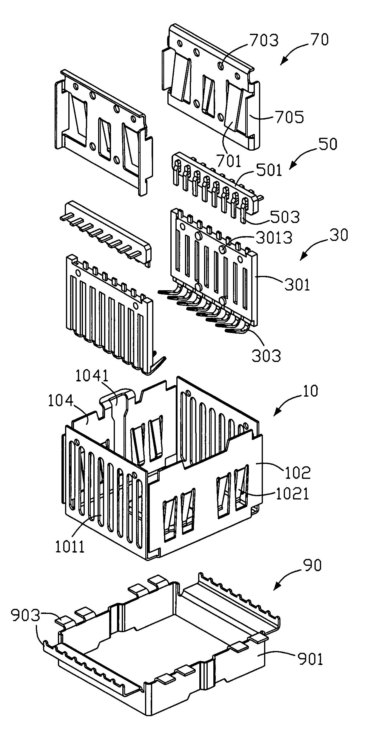
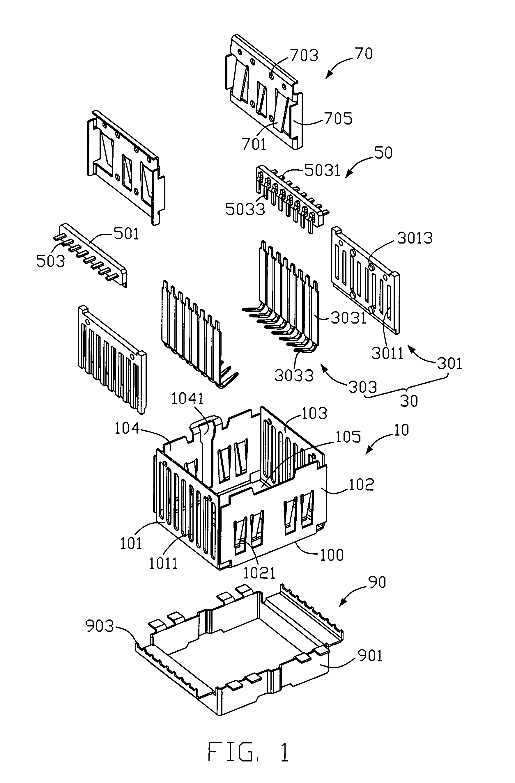
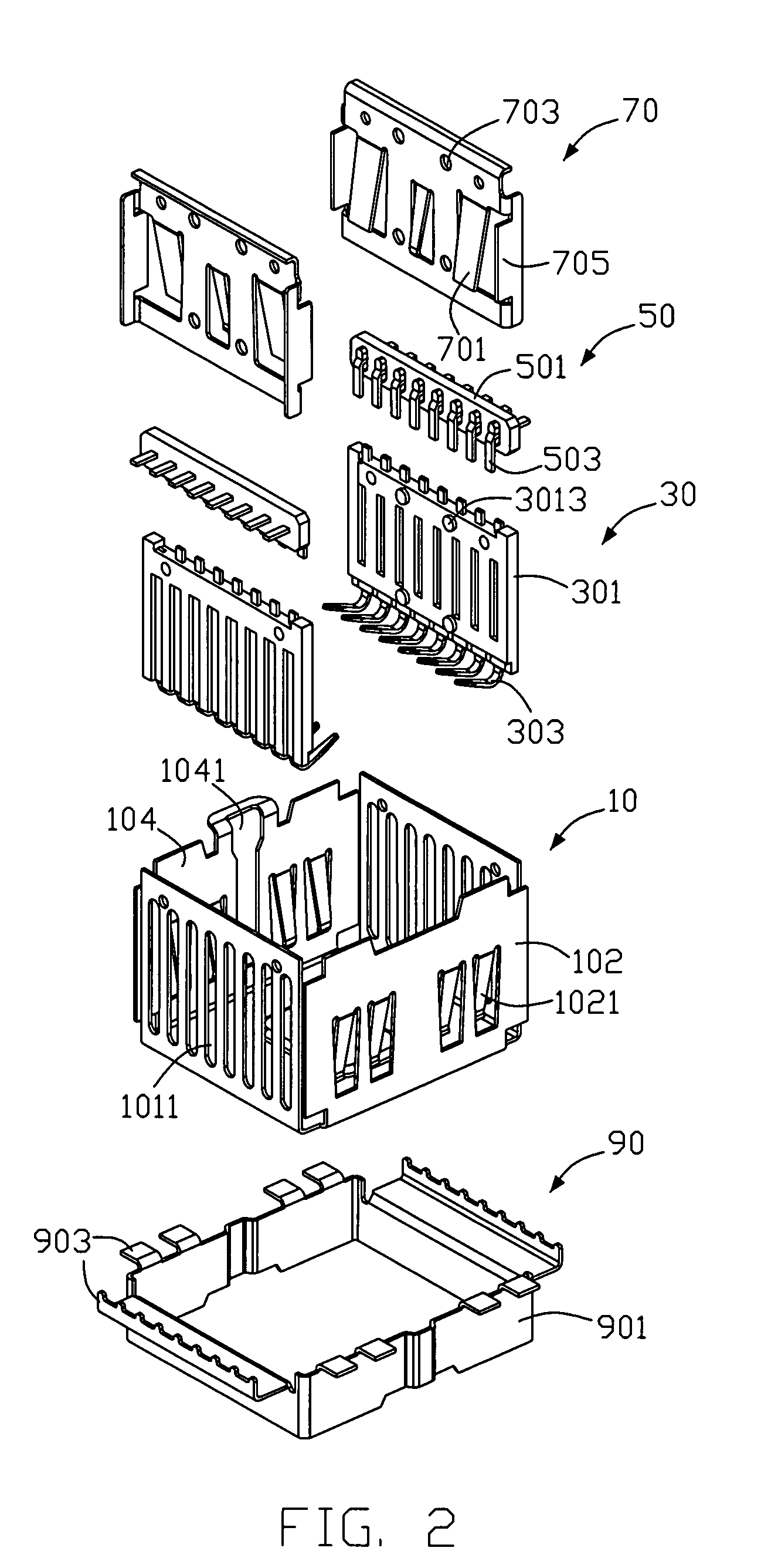
[0026]A shield connector according to the present invention is applicable to an electronic apparatus such as digital cameras, PDAs (Personal Digital Assistants), PCs (Personal Computers), mobile phones or the like. In the preferred embodiment illustrated in FIGS. 1-8, the shield connector 1 is illustrated as to be used in a mobile handset (not shown) for connecting a camera module (not shown) to a PCB (not shown).
[0027]FIG. 1 is an exploded perspective view of the shield connector for receiving a camera module in the embodiment of this invention. In the figure, the reference numeral 10 denotes a housing made of a metal material. The reference numeral 30 denotes a pair of contact module. The reference numeral 50 denotes a pair of soldering assembly. The reference numeral 70 denotes a pair of shield piece made of metal material. The reference numeral 90 denotes a movable shell assembled on the outer surface of the housing.
[0028]As shown in FIGS. 1-3, the housing 10 includes a plane shaped bottom plate 100 and box shaped insulating member having surrounding wall plates 101, 102, 103, and 104. And said bottom plate 100 and the surrounding wall plate 101, 102, 103, and 104 together jointly defines a receiving space 105 to receive the camera module.
[0029]Also referring to the FIGS. 1-3, a plurality of narrow openings 1011 are defined in the surrounding wall plate 101, 103 at a predetermined interval and run through the inner surface to the outer surface thereof. Therefore, the soldering assembly 50 can be attached to the contact module 30 via said narrow openings 1011 when the contact module 30 assembled on the housing 10.
[0030]The surrounding wall plates 101, 102, 103, and 104 extend perpendicular from the edge portion formed on the bottom plate 100, respectively. A plurality of spring fingers 1021 is formed on the inner surface of the surrounding wall plate 102, 104 and extends into a center of the housing 10 so as to provide ground contact to the camera module. Wherein a window 1041 is defined in one surrounding wall plate 104 for engaging with a corresponding portion of the camera module. When the camera module is inserted into the housing 10 from above, the corresponding portion of the camera module protrudes outwardly via the window 1041 of the housing 10, by this arrangement, the camera module can be fitted into the housing 10 correctly.
[0031]Also please referring to the FIGS. 1-3 and combine to the FIGS. 4, 9, 11, the contact module 30 includes an insulating part 301and a plurality of terminal contacts 303 insert-molded into the insulating part 301. A plurality of contact inserting slots 3011 is defined in the insulating part 301 and penetrates the insulating part 301 along the thickness direction. Said contact inserting slots 3011 are located on a corresponding position with the narrow opening 1011 of the housing 10. In additional, several ribs 3013 are formed on one surface of the insulating part 301 to engage with the shielded piece 70.
[0032]Each terminal contact 303 includes a base portion 3031 extending perpendicular and a contact portion 3033 disposed above the bottom plate 100 of the housing10. Each terminal contact 3033 is attached to the insulating part 303 with the base portion 3031 insert-molded into the insulating part 301. Moreover, the width of the base portion 3031 is broader than the contact portion 3033 to increase the resilient property of the contact portion 3033.
[0033]It can be noted that said terminal contact 303 only has a base portion 3031 and a contact portion 3033 and does not has a soldering portion connected with a printed circuit board 2. The reason will be described in the following paragraphs.
[0034]Also please referring to the FIGS. 1-3 and combine to the FIGS. 4, 9, 11, the soldering assembly 50 attached to the contact module 30 and comes to solder with the printed circuit board 2, which comprising a plurality of soldering member 503 and a holding member 501 for fixing said soldering member 503. As shown in the FIGS. 1-3, 9, 11 especially, each soldering member 503 configured as an L-shape configuration, comprising an attaching portion 5033 attached to the terminal contact 303 and a soldering portion 5031 to be soldered to the printed circuit board 2. As a result, the soldering member 503 can be attached to the terminal contact 303 at any position within the range so as to meet with the different demands of the mobile phone. By the provision of the current invention, it is not necessary to use a different electrical connector with the different demand of the mobile phone. In other word, present electrical connector can be applied in different mobile phones.
[0035]Also please referring to the FIGS. 1-3, the shield pieces 70 cover on the contact module 30 separately and made of a metal sheet. A plurality of locking fingers 701 extends slantly away an inner surface thereof. A plurality of aligning holes 703 is formed corresponding to the ribs 3013 of the insulating part 301, by which the shield pieces 70 and the insulating part 301 are assembled together. Additional, a pair of wings 705 are formed on the two side ends of each shield piece 70, which perpendicular to the surface of the shield piece 70 so as to make the wing 705 attach to a corresponding portion of the inner surface of the surrounding wall plate 102, 104.
[0036]The shield connector 1 further includes a movable shell 90 attached to the housing 10 and soldered with the printed circuit board 2. It is bent from a metal sheet to a rectangle shape and is composed of four walls 901. The inner surface of the walls 901 abuts against the outside surface of the housing 10. A plurality of soldering pads 903 are formed on the top or below end of the walls 901 of the movable shell 90 and extends outwardly thereof so as to contact with the electrically pads formed on the printed circuit board 2. It can be noticed that, in the FIG. 1, the movable shell 90 is a rectangular configuration; while it is all right that the movable shell 90 is composed of a pair of metal shell. When the movable shell 90 assembled with the housing 10, they are assembled together by spot-welding at the position, which the wings 703 of the shielded piece are located.
[0037]Referring to FIGS. 1-11, in assembly, firstly, the terminal contacts 30 are insert-molded into the insulating part 301 with the base portion 3031 being set in the contact insert slots 3011 thereof, by which the contact module 30 are assembled together; secondly, the shield piece 70 covered on the contact modules 30 with the ribs 3013 of the insulating part 301 being inserted into the aligning holes 703 of the shield piece 70; thirdly, the shield pieces 70 and the contact module 30 are together mounted on the first and third surrounding wall plate 101, 103 of the housing 10 separately with the wing 705 resisting the inner surface of the second and fourth surrounding wall plate 102, 104 of the housing 10 and the contact portion 3033 of the terminal contact 303 disposed above the bottom plate 100 of the housing 10; fourthly, the soldering assembly 50 are anchored on the outer surface of the first and third surrounding wall plate 101, 103 and contacts to the terminal contact 303 with attached portion 5033 thereof attached to the base portion 3031 of the terminal contact 303 via the narrow opening 1011 and the soldering portion 5031 extending outward from the housing 10 so as to connect to the printed circuit board 2; finally, the movable shell 90 covered on the outer surface of the housing 10 from above/below and the inner surface of the wall of the movable shell 90 against with the outer surface of the housing 10, meanwhile, the soldering pads 903 located on a same height of the soldering portion 5031 of the soldering assembly 50 so as to provide a steady electrical connection between the shield connector 1 and the printed circuit board 2.
[0038]It can be noticed that, in the above description, the movable shell 90 assembled with the housing 10 from above, while it is all right that the movable shell 90 assembled with the housing 10 from below as shown in FIGS. 7-11. It is the key factor that how to make the movable shell 90 attach to the housing 10 firmly. For example, if the soldering portion 5031 of the soldering assembly 50 located on a position adjacent to the upper portion of the first and third surrounding wall plate 101, 103, the movable shell 90 assembled with the housing 10 from the below and the soldering pads 903 of the movable shell 90 located on the upper edge thereof, because the movable shell 90 hardly contacted with the housing 10 firmly if it assembled with the housing 10 from above. On the contrary, if the soldering portion 5031 located on a position adjacent to the lower portion of the first and third surrounding wall plate 101, 103, the movable shell 90 assembled with the housing 10 from above.
[0039]In the above description of the preferred embodiment, a contact section and a soldering section of the terminal contact located on separate elements, in other word, the contact portion for coming to contact with the pads formed on the bottom surface of the camera module defined in the terminal contact and the soldering portion for connecting with the printed circuit board 2 defined in the soldering assembly. Consequently, the soldering section can be attached to any position of the terminal contact so as to satisfy the different demand of the mobile phone.
[0040]It is to be understood, however, that even though numerous, characteristics and advantages of the present invention have been set fourth in the foregoing description, together with details of the structure and function of the invention, the disclosed is illustrative only, and changes may be made in detail, especially in matters of number, shape, size, and arrangement of parts within the principles of the invention to the full extent indicated by the board general meaning of the terms in which the appended claims are expressed.

PUM

no PUM

Description & Claims & Application Information

We can also present the details of the Description, Claims and Application information to help users get a comprehensive understanding of the technical details of the patent, such as background art, summary of invention, brief description of drawings, description of embodiments, and other original content. On the other hand, users can also determine the specific scope of protection of the technology through the list of claims; as well as understand the changes in the life cycle of the technology with the presentation of the patent timeline. Login to view more.
Why Eureka
Try Eureka