

EMI filter terminal assembly with wire bond pads for human implant applications
a technology of filter terminals and wire bond pads, which is applied in the direction of feed-through capacitors, artificial respiration, therapy, etc., can solve the problems of serious interference with the proper operation of the pacemaker, dangerous or life-threatening for the patient dependent on the pacemaker, etc., to prevent cracking of ceramic capacitors, increase the beam moment of inertia, and increase the beam height
- Summary
- Abstract
- Description
- Claims
- Application Information
AI Technical Summary
Benefits of technology
Problems solved by technology
Method used
Image

Examples
Embodiment Construction
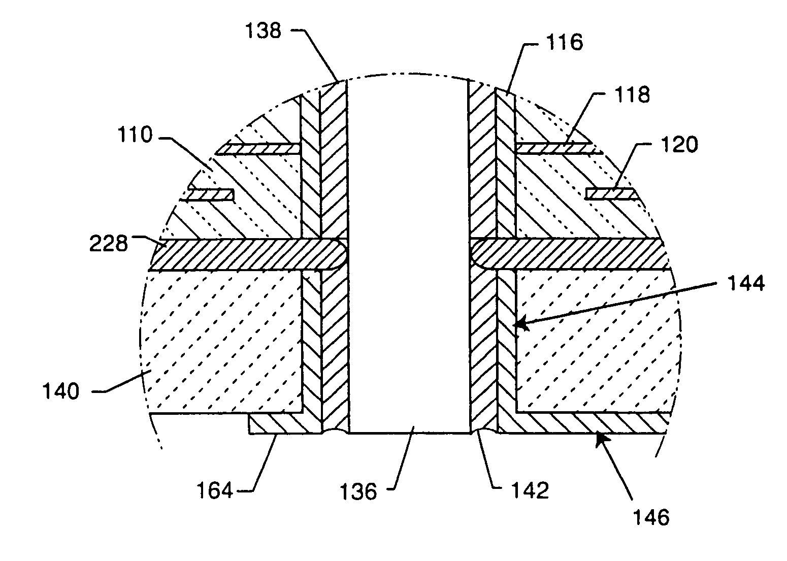
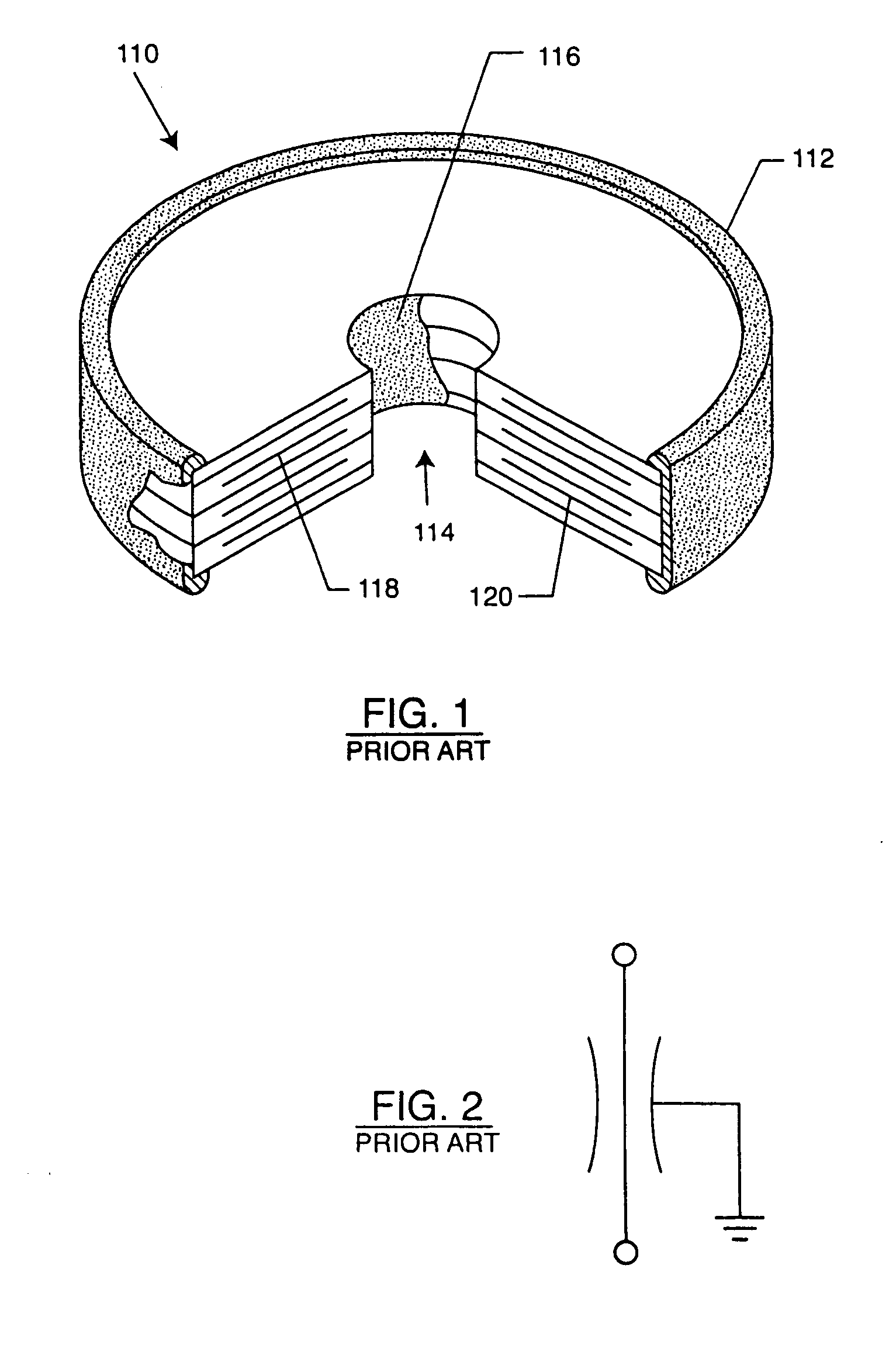
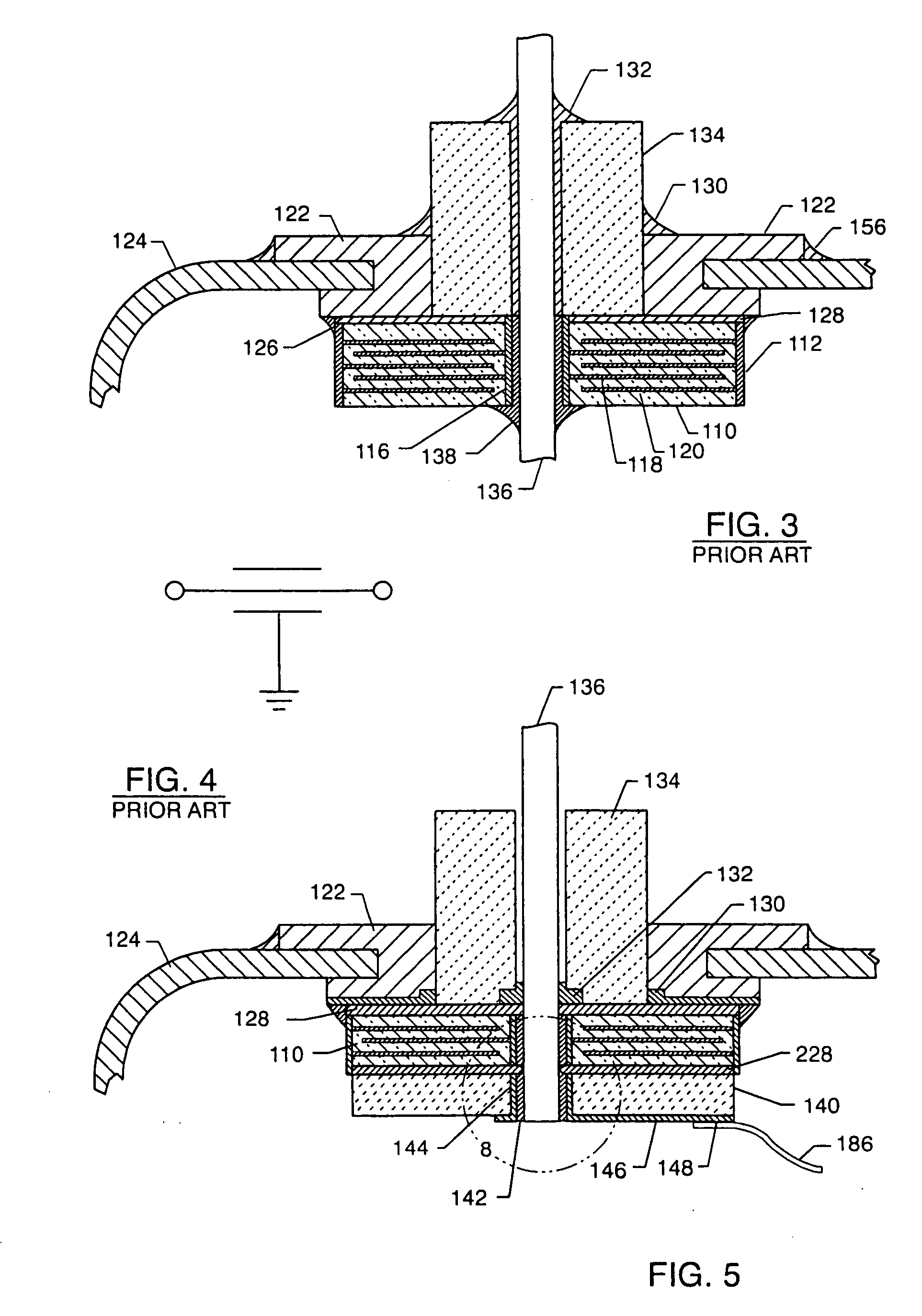
[0126] Reference will now be made in detail to presently preferred embodiments of the invention, examples of which are represented in the accompanying drawings for purposes of illustration. Such examples are provided by way of an explanation of the invention, not a limitation thereof. In fact, it will be apparent to those skilled in the art that various modifications and variations can be made in the present invention, without departing from the spirit and scope thereof. For instance, figures illustrated or described as part of one embodiment can be used on another embodiment to yield a still further embodiment. Still further, variations and selection of materials and / or characteristics may be practiced, to satisfy particular desired user criteria. Thus, it is intended that the present invention cover such modifications and variations as come within the scope of the present features and their equivalents. In the following description, functionally equivalent components of the variou...
PUM
 Abstract
Description
Claims
Application Information