Methods of making microelectronic assemblies including compliant interfaces
What is AI technical title?
AI technical title is built by Patsnap AI team. It summarizes the technical point description of the patent document.
a microelectronic assembly and interface technology, applied in the direction of dielectric characteristics, printed circuit aspects, printed element electric connection formation, etc., can solve the problem that the vertical height of the pads cannot be extremely uniform, and achieve the effect of reducing the stress on the connections therebetween and effective encapsulation barrier against moisture and contaminants
Inactive Publication Date: 2005-06-30
TESSERA INC
View PDF70 Cites 20 Cited by
Summary
Abstract
Description
Claims
Application Information
AI Technical Summary
This helps you quickly interpret patents by identifying the three key elements:
Problems solved by technology
Method used
Benefits of technology
Benefits of technology
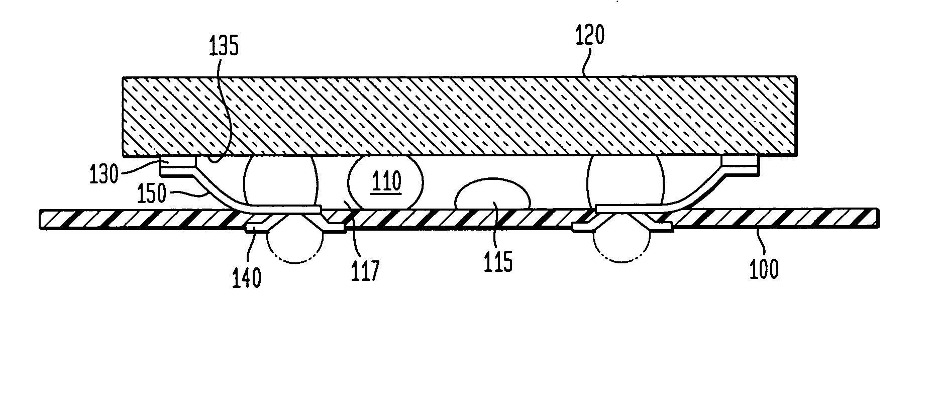
[0015] The pads or the pad / injected elastomer combination provide a compliant, planar interface which effectively accommodates for the thermal coefficient of expansion mismatch between the chip and a supporting substrate thereby alleviating much of the stress on the connections therebetween. Further, the combination provides an effective encapsulation barrier against moisture and contaminants.
Problems solved by technology
At this stage of the process, the vertical height of the pads need not be extremely uniform.
Method used
Image
Click on the blue label to locate the original text in one second.
Reading with bidirectional positioning of images and text.
Examples
Embodiment Construction
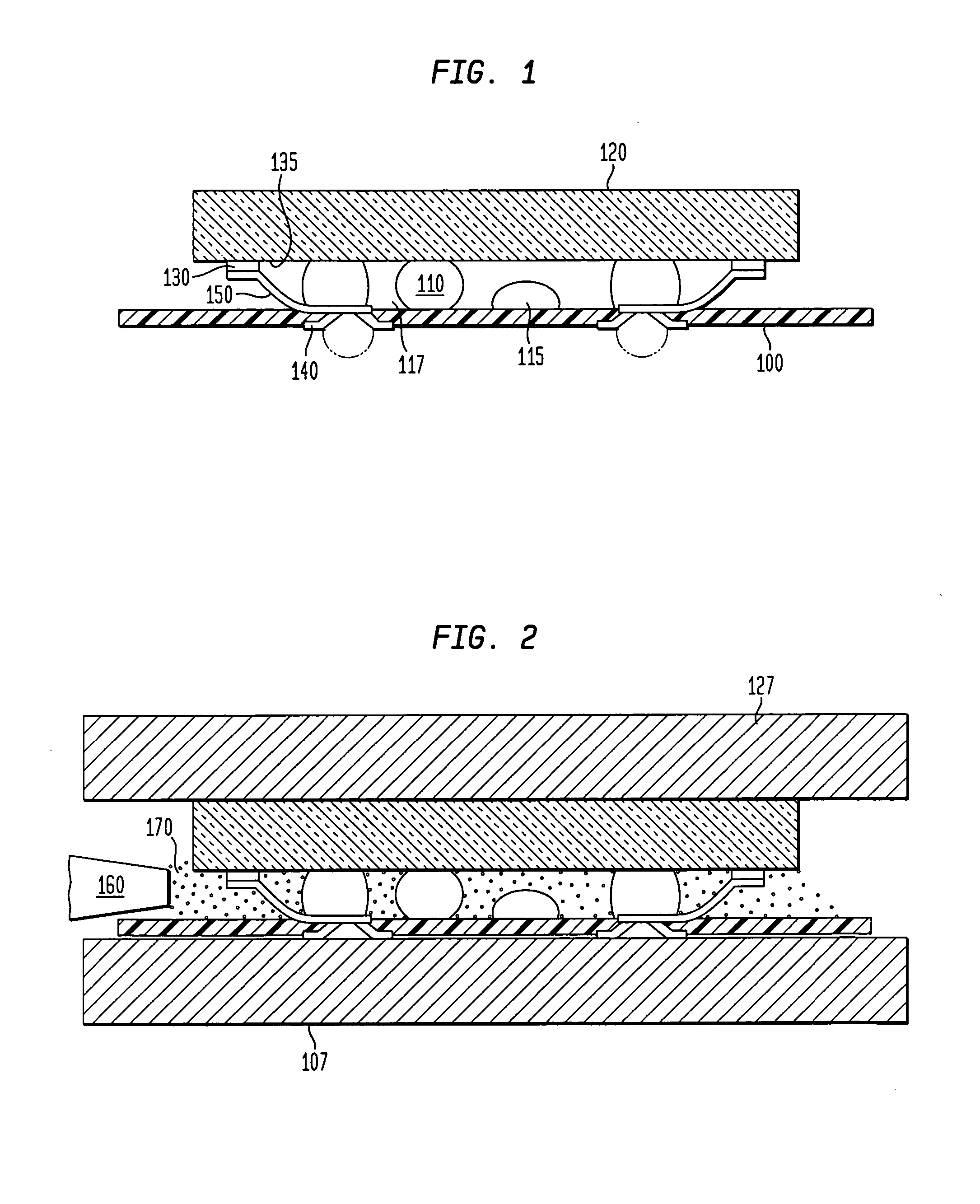
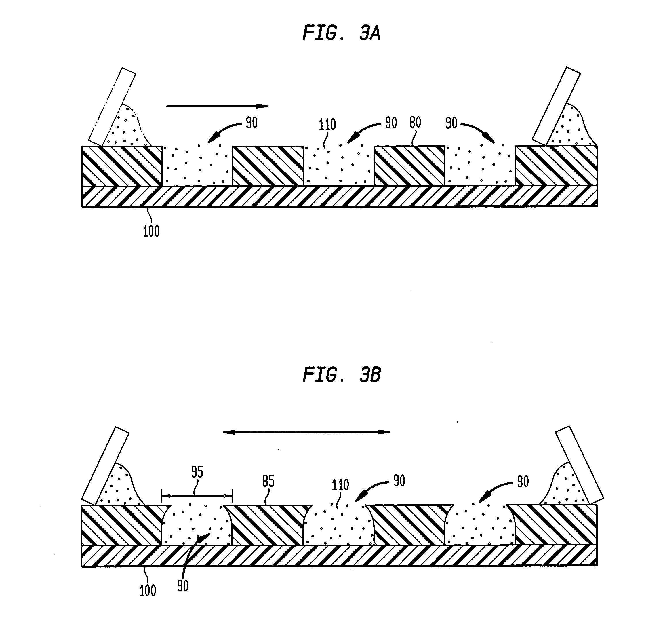
[0026]FIGS. 1 and 2 show a side view of a chip size package embodiment, according to the present invention. A support structure 100 is provided having a first and a second surface. The support structure 100 may be substantially rigid, semi-rigid or flexible. However typically, the support structures 100 is comprised of a flexible, but substantially inextensible, dielectric film, preferably formed from a polymeric material, such as KAPTON™“E” available from DuPont Chemical Corp., of an approximate thickness between 25 microns and 75 microns. Further, the dielectric film 100 typically has conductive terminals 140 on its second surface.
[0027] A porous layer, such as a layer of a plurality of compliant pads 110, is attached to the first surface of the film 100. The compliant pads 110 are typically made of an curable liquid elastomer material, such as the Dow Corning silicone elastomer 577, known as “Sylgard™”, with about 5-10% of fumed silica in order to obtain a stiff, thixotropic con...
PUM
Abstract
An assembly includes a structure, a plurality of terminals and a plurality of compliant pads disposed between said terminals and said structure. The terminals are aligned with at least some of said pads, with the pads providing a standoff between the structure and the terminals. The compliant pads are preferably made of a non-conductive material such as a silicone elastomer.
Description
CROSS REFERENCE TO RELATED APPLICATIONS [0001] This application is a continuation of U.S. patent application Ser. No. 10 / 123,547, filed Apr. 16, 2002, which application is a continuation of U.S. patent application Ser. No. 09 / 517,852, filed Mar. 2, 2000, now U.S. Pat. No. 6,525,429, which is a divisional of U.S. patent application Ser. No. 08 / 842,313, filed Apr. 24, 1997, now U.S. Pat. No. 6,133,639, which in turn is a divisional of U.S. patent application Ser. No. 08 / 365,699, filed Dec. 29, 1994, now U.S. Pat. No. 5,659,952, which in turn is a continuation-in-part of U.S. patent application Ser. No. 08 / 309,433, filed Sep. 20, 1994, now abandoned, the disclosures of which are hereby incorporated by reference herein.FIELD OF THE INVENTION [0002] The present invention relates, generally, to providing a compliant interface for a semiconductor chip, and more particularly relates to a method and apparatus for providing a compliant interface to accommodate for differences in the thermal c...
Claims
Application Information
Patent Timeline
Application Date:The date an application was filed.
Publication Date:The date a patent or application was officially published.
First Publication Date:The earliest publication date of a patent with the same application number.
Issue Date:Publication date of the patent grant document.
PCT Entry Date:The Entry date of PCT National Phase.
Estimated Expiry Date:The statutory expiry date of a patent right according to the Patent Law, and it is the longest term of protection that the patent right can achieve without the termination of the patent right due to other reasons(Term extension factor has been taken into account ).
Invalid Date:Actual expiry date is based on effective date or publication date of legal transaction data of invalid patent.
Patent Type & AuthorityApplications(United States)

