Low loss substrate for integrated passive devices

Active Publication Date: 2010-06-10
NXP USA INC
View PDF12 Cites 21 Cited by
  • Summary
  • Abstract
  • Description
  • Claims
  • Application Information

AI Technical Summary

Benefits of technology

[0036]Referring now to manufacturing stage 126 of FIG. 26, layer 82″ of thickness 81″ analogous to layer 82 of FIG. 15 is formed over structure 225, thereby filling void trenches 74″ of width 80″ and creating inclusions 83″ of width 80″ in much the same manner as described for void trenches 74 and inclusions 83 of manufacturing stage 115 of FIG. 15, the discussion of which is incorporated herein by reference. Structure 226 results. While manufacturing stage 126 of FIG. 26 illustrates the situation where mask 72 is left in place during deposition of layer 82″, in other embodiments, mask layer 72 may be removed prior to such deposition. Either arrangement or sequence is useful. Referring now to manufacturing stage 127 of FIG. 27, structure 226 is planarized in much the same manner as has been previously described in connection with manufacturing stage 116 of FIG. 16, the discussion of which is hereby incorporated by reference. Structure 227 results. Advantage is taken of the presence of further pad layer 70 which provides a convenient planarization polish stop and/or etch stop. Structure 227 is then subjected to manufacturing stages analogous to manufacturing stages 117-120 of FIGS. 17-20, the discussion of which is incorporated herein by reference, culminating in manufacturing stage 128 of FIG. 28 analogous to manufacturing stage 120 of FIG. 20, with the difference that residual SC substrate columns or pillars 92″ of width 93″ and center-to-center spacing 94″ are incorporated in CDR 62″ of electronic element 44″. Poly inclusions 65″ of width 80″ and separation 89″ and center-to-center distance 66″ are provided in deposited dielectric regions 78″ having therein substantially un-oxidized substrate columns 92″. Poly-inclusions 65″ are electrically floating and residual substrate columns 92″ are separated from IPD 35 by at least portions 70″ and 68″ of pad layers 70, 68 and layer 86, thereby limiting their impact on the E-M coupling field generated by IPD 35. Active device 47 (or 24 or of any other type) can be formed before, during or after formation of CDR 62″ and IPD 35.
[0037]A particular advantage of the invented embodiments, is that CDR 62, 62′, 62″ can be formed early in the process flow prior to the principal steps needed for forming the active device(s) in ADR region 46. This means that the device regions need not be exposed to t

Problems solved by technology

The performance and cost of many devices, especially radio frequency (RF) power devices and integrated circuits (ICs), are particularly sensitive to losses and layout rules associated with such integrated passive devices and to their occupied area.
Electro-magnetic (E-M) coupling of IPDs to the semiconductor substrates on which they are formed can give rise to eddy current losses in the substrate that can degrade overall device and IC performance.
These problems become more severe with high periphery and higher frequency devices.
When the IPDs incorporate resonant elements (e.g., inductors, capacitors, transmission lines, filters, etc.) the E-M coupling between such IPDs and the underlying semiconductor substrate can degrade the “Q” o

Method used


Image

  • Low loss substrate for integrated passive devices
  • Low loss substrate for integrated passive devices
  • Low loss substrate for integrated passive devices

Examples


first embodiment

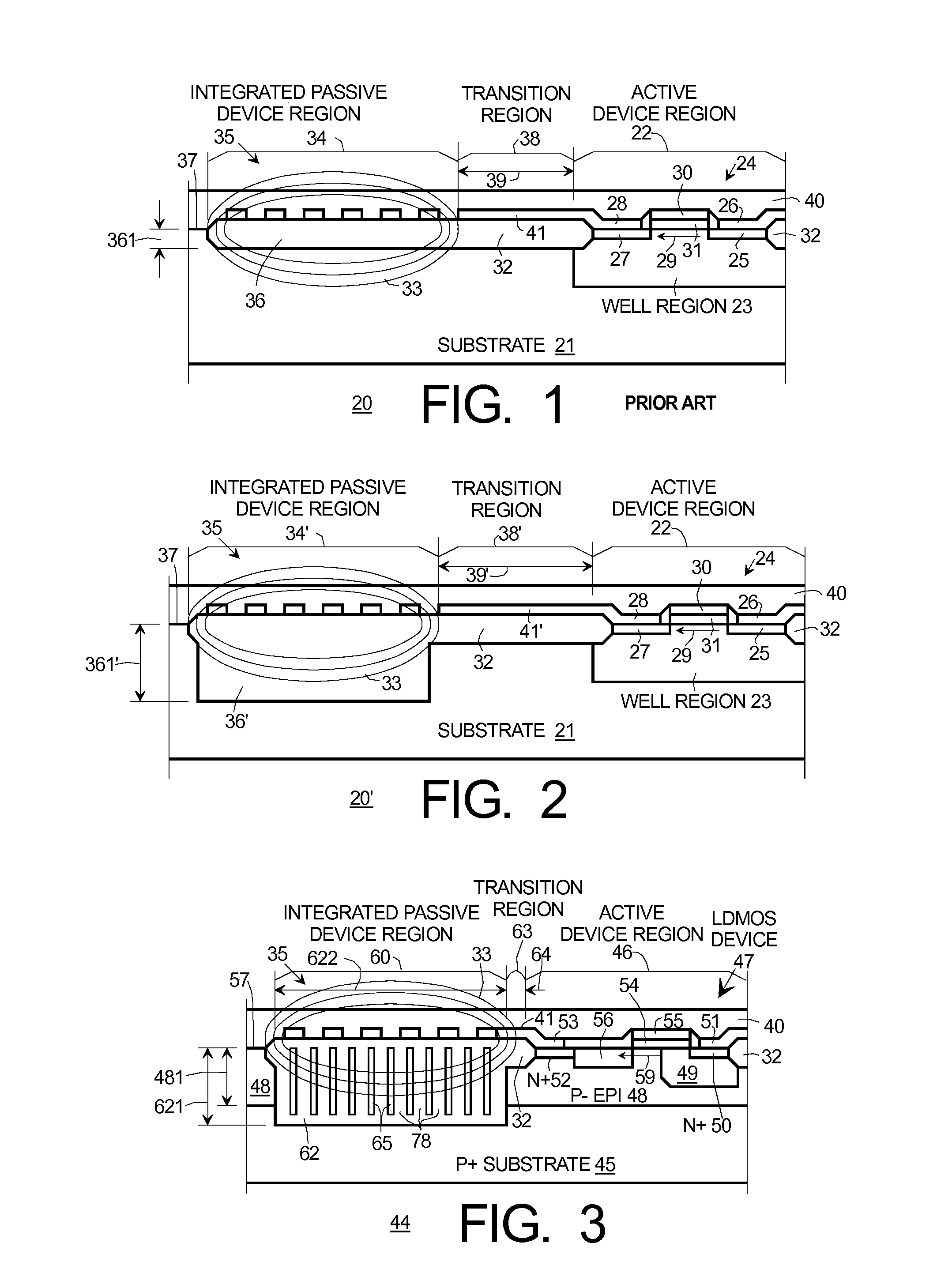
[0038] there is provided a method (112-128) for forming an electronic element (44, 44′, 44″) incorporating an integrated passive device (IPD) (35) and an active device (24, 47), comprising, providing (112, 121, 124) a substrate (45) of a first material having a first thermal expansion coefficient (TEC) and having a first surface (57), wherein the substrate (45) has therein a first portion (46) adapted to receive the active device (24, 47) and a second portion (60) adapted to receive the IPD (35), forming (112, 121, 124) a mask (72) on the second portion (60), the mask having spaced-apart openings (73, 73′, 73″) of a first width (75, 75′, 75″), etching spaced-apart trenches (74, 74′, 74″) of substantially the first width (75, 75′, 75″) to a first depth (741, 741″) in the substrate (45), leaving columns (76, 76′, 76″) of substantially undisturbed substrate (45) material between the trenches (74, 74′, 74″) and other portions of the substrate (45) material beneath the trenches (74, 74′,...

second embodiment

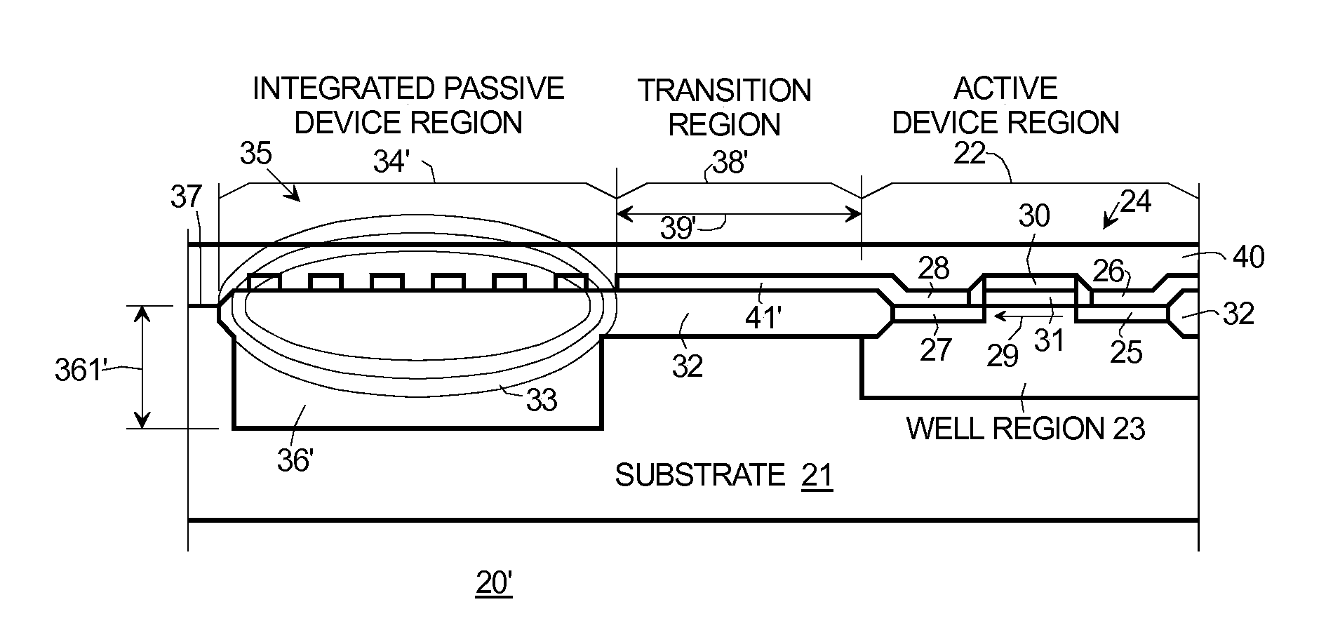
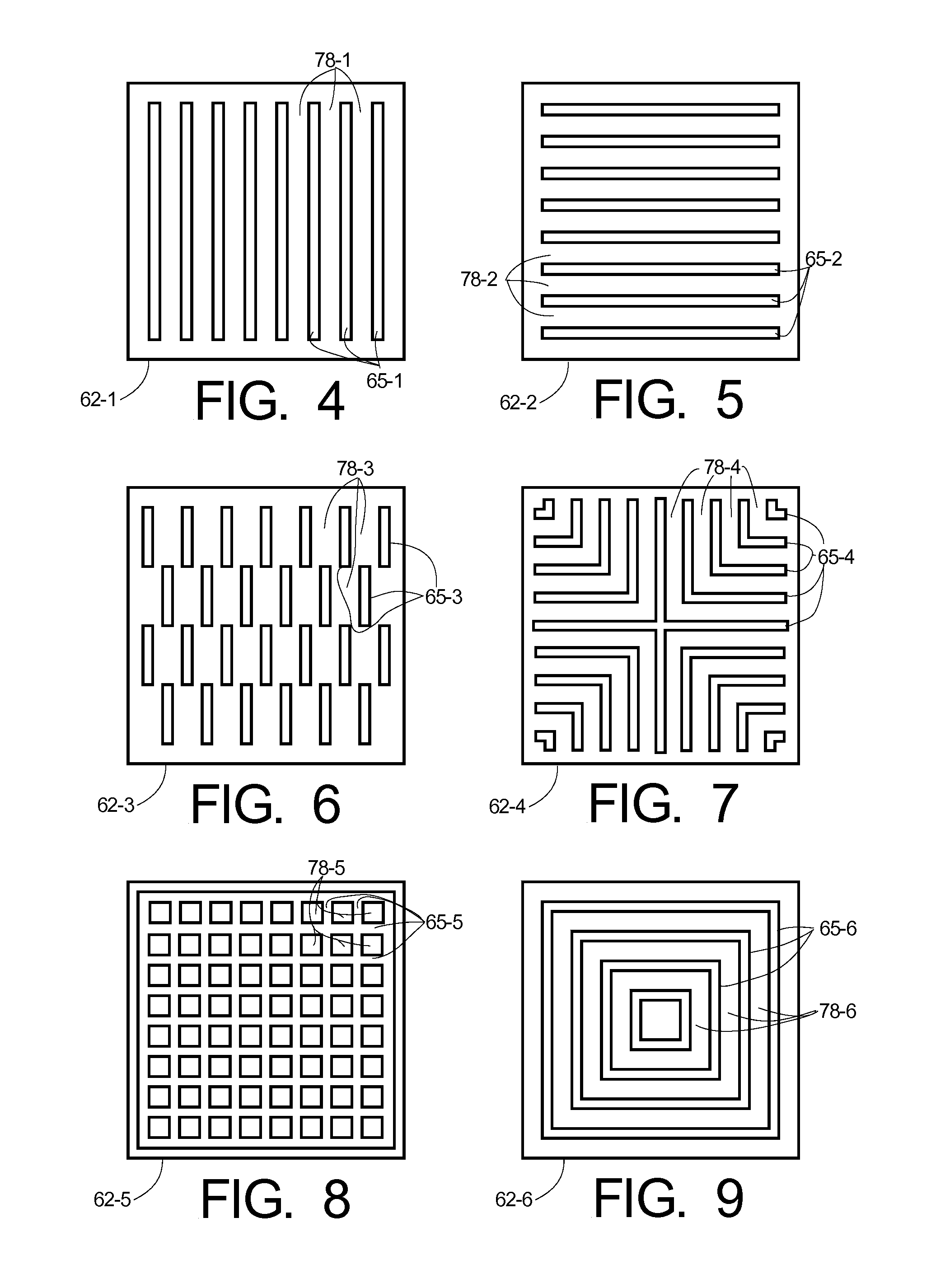
[0039] there is provided an electronic assembly (44, 44′, 44″), comprising, a semiconductor (SC) substrate (45) having a first thermal expansion coefficient (TEC) and an active device region (46) and an integrated passive device (IPD) region (60), an integrated passive device (IPD) (35) located in the IPD region (60), a region of an insulating material (78, 78′, 78″) having a second TEC, located in the IPD region (60) and adapted to support the IPD (35), and inclusions (65, 65′, 65″) of a further material (82) within the region of insulating material (78, 78′, 78″) thereby forming a composite dielectric region (62, 62′, 62″), wherein the further material (82) has a third TEC less than the second TEC, and wherein the inclusions (65, 65′, 65″) are electrically isolated from the substrate (45) and the IPD (35). According to a further embodiment, the inclusions have a width (80, 80′, 80″) in the range of about 0.2 to 5 micrometers. According to a still further embodiment, the inclusions...

third embodiment

[0040] there is provided an electronic assembly (44, 44′, 44″), comprising, a semiconductor substrate (45) comprising silicon, with an active device region (46) and an integrated passive device (IPD) region (60) thereon, a composite dielectric region (62, 62′, 62″) located in the IPD region (60), comprising silicon oxide regions (78, 78′, 78″) with electrically isolated polysilicon or amorphous silicon inclusions (65, 65′, 65″) therein, an integrated passive device (IPD) (35) located above the composite dielectric region (62, 62′, 62″) in the IPD region (60), and an active device (24, 47) located in the active device region (46) and electrically coupled to the IPD (35). According to a further embodiment, the IPD region (60) and the active device region (46) are laterally separated by less than 100 micrometers. According to a still further embodiment, the IPD region (60) and the active device region (46) are laterally separated by less than about 50 micrometers. According to a yet fu...


PUM


Abstract

Electronic elements (44, 44′, 44″) having an active device region (46) and integrated passive device (IPD) region (60) on a common substrate (45) preferably include a composite dielectric region (62, 62′, 62″) in the IPD region underlying the IPD (35) to reduce electromagnetic (E-M) (33) coupling to the substrate (45). Mechanical stress created by plain dielectric regions (36′) and its deleterious affect on performance, manufacturing yield and occupied area may be avoided by providing electrically isolated inclusions (65, 65′, 65″) in the composite dielectric region (62, 62′, 62″) of a material having a thermal expansion coefficient (TEC) less than that of the dielectric material (78, 78′, 78″) in the composite dielectric region (62, 62′, 62″). For silicon substrates (45), non-single crystal silicon is suitable for the inclusions (65, 65′, 65″) and silicon oxide for the dielectric material (78, 78′, 78″). The inclusions (65, 65′, 65″) preferably have a blade-like shape separated by and enclosed within the dielectric material (78, 78′, 78″).

Description

FIELD OF THE INVENTION[0001]The present invention generally relates to semiconductor (SC) devices and integrated circuits (ICs) and their methods of manufacture, and more particularly, structures and methods for providing SC devices and ICs embodying low loss integrated passive devices on a common substrate.BACKGROUND OF THE INVENTION[0002]A need continues to grow for more complex semiconductor (SC) devices and integrated circuits (IC) incorporating integrated passive devices. Non-limiting examples of such passive devices are inductors, capacitors, resistors, interconnections, transmission lines, baluns, couplers, filters, various other high frequency components, and so forth. For manufacturing and performance efficiency it is advantageous to form the passive devices on the same substrate as the transistors and / or other active devices used to implement the desired electronic function. Hence, the description “integrated passive devices”, abbreviated as “IPD”.[0003]The performance and...

Claims


Application Information

Patent Timeline
IPC IPC(8): H01L29/78H01L21/76H01L27/00
CPCH01L21/763H01L27/0207H01L28/10H01L27/0629H01L27/08H01L27/0617
Inventor REN, XIAOWEIBURGER, WAYNE R.KERR, COLINBENNETT, MARK A.
Owner NXP USA INC
Why Eureka
Try Eureka