3-d circuits with integrated passive devices

a passive device and integrated circuit technology, applied in semiconductor devices, semiconductor/solid-state device details, diodes, etc., can solve the problems of increasing thermal impedance between power amplifier active device (ad) regions, limiting the gain and efficiency of high-frequency power amplifiers, and difficult to create effective 3-d ics incorporating high-frequency power amplifiers

Active Publication Date: 2010-05-27
INVENSAS CORP
View PDF27 Cites 116 Cited by
  • Summary
  • Abstract
  • Description
  • Claims
  • Application Information

AI Technical Summary

Problems solved by technology

This is especially true of devices and circuits that operate at high frequencies where there is often a need to include integrated passive devices (e.g., inductors, capacitors, resistors, transmission lines, ground planes, shielding structures, baluns, etc.) that cannot easily be provided as a part of the associated semiconductor devices.
Creating effective 3-D ICs incorporating high frequency power amplifiers has proved especially difficult because of electromagnetic (EM) cross-talk among the various components and higher than desired losses arising from stray electromagnetic (EM) fields inducing undesirable eddy currents in underlying semiconductor substrates.
These effects can limit the gain and efficiency of high frequency power amplifiers.
However, use of thicker substrates creates other problems, such as for example, increased thermal impedance between power amplifier active device (AD) regions on or near a front face of the substrate and a heat sink coupled to a rear face of the substrate.
This increased thermal impedance can degrade overall performance.
Thus, power amplifier ICs embodying IPDs involve conflicting requirements.
However, there are physical limits on the number and thickness of multilayer dielectric-metal stacks for IPDs that can be deposited on a semiconductor substrate containing active devices (ADs).
This can make it difficult or impossible, for example, to reduce the cross-talk among the IPDs and / or between the IPDs and the underlying ADs and their substrate.

Method used


Image

  • 3-d circuits with integrated passive devices
  • 3-d circuits with integrated passive devices
  • 3-d circuits with integrated passive devices

Examples


first embodiment

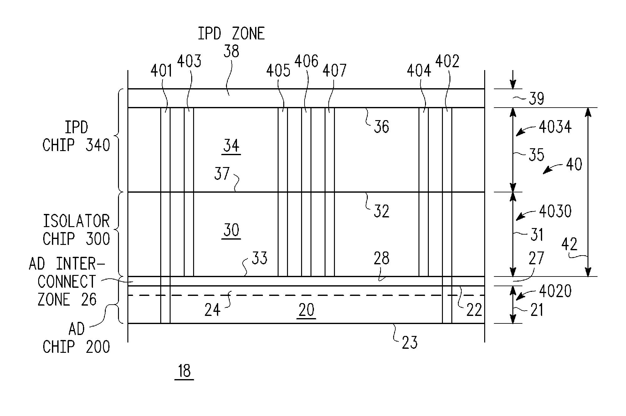
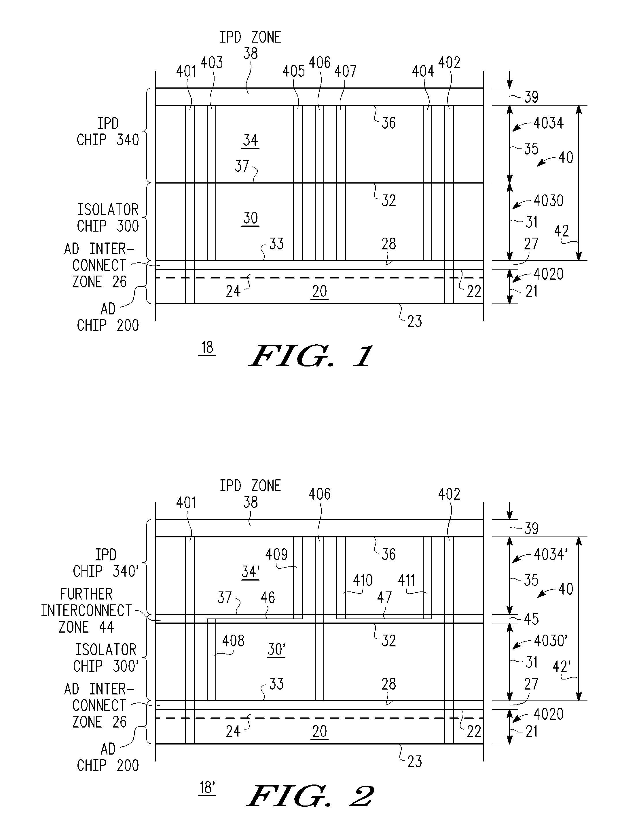
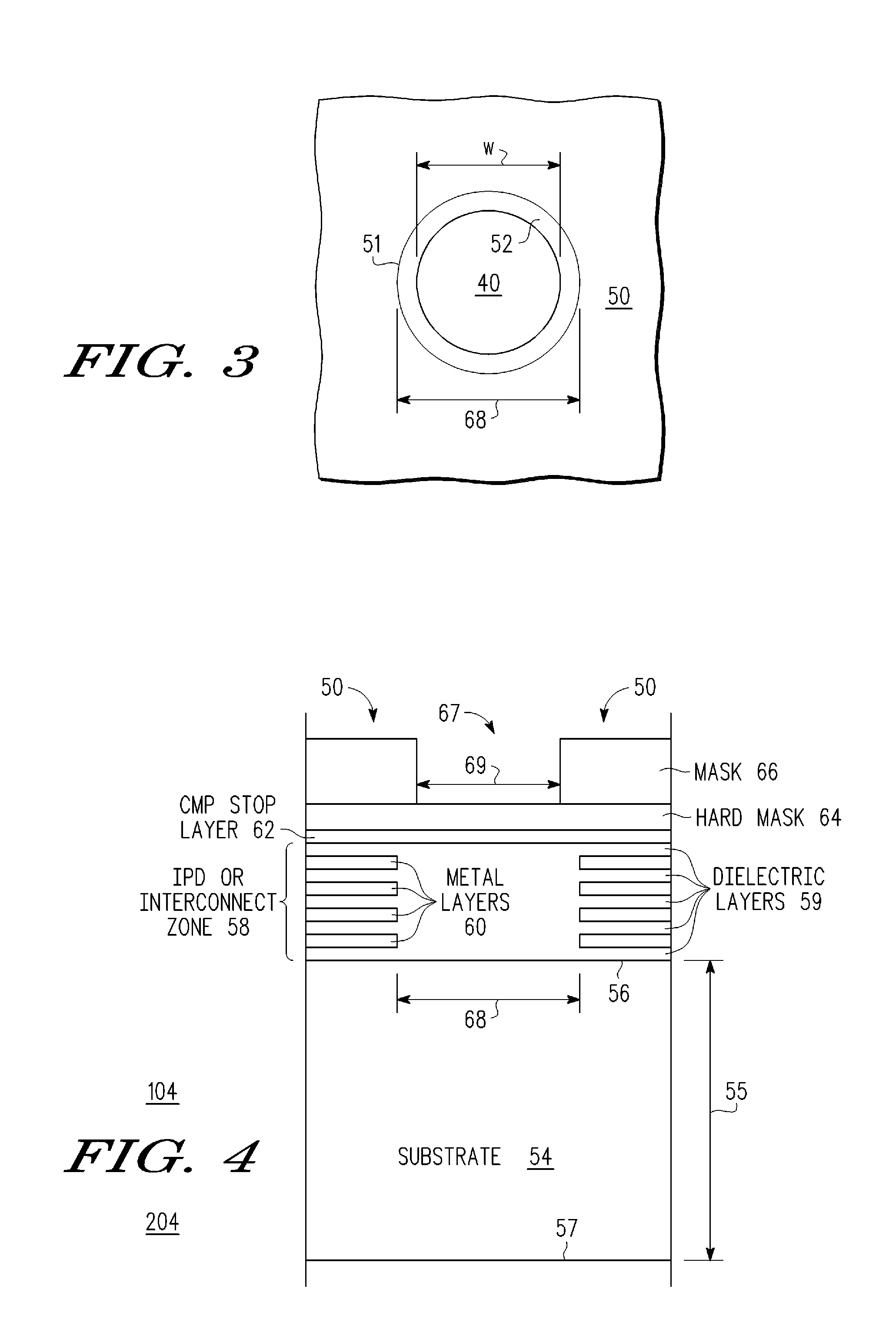
[0034] there is provided a 3-D integrated circuit (IC) (90, 18, 18′), comprising, an active device (AD) substrate (20) having an AD region (26) thereon with device contacts therein, an isolator substrate (30), separately formed from the AD substrate (20) and having one or more through-substrate-vias (TSVs) (4030) therein adapted to be coupled to one or more of the device contacts in the AD region (26) of the AD substrate (20), and an integrated passive device (IPD) substrate (34), separately formed from the AD substrate (20) and the isolator substrate (30) and having an IPD zone (38) on its surface in which IPDs have been formed, and having one or more TSVs (4034) there through, adapted to couple one or more of the IPDs in the IPD zone (38) to TSVs (4030) in the isolator substrate (30). According to a further embodiment, at least some of the TSVs (4030) in the isolator substrate (30) are coupled to some of the device contacts in the AD region (26) on the AD Substrate (20). According...

second embodiment

[0035] there is provided a method for forming a 3-D integrated circuit (IC) (90, 18, 18′), comprising, forming on separate substrates (20, 30, 34) at least an active device chip (200), an isolator chip (300) and an integrated passive device (IPD) chip (340), wherein at least two of such chips (200, 300, 340) have one or more conductor filled vias (40) extending there through and wherein at least some vias in the IPD chip (340) are coupled to one or more integrated components on the IPD chip (340), stacking the active device chip (200), the isolator chip (300) and the IPD chip (340) so that a first via in a first of the at least two chips is aligned with a second via in another of the at least two chips; and bonding the active device chip (200), the isolator chip (300) and the integrated passive device (IPD) chip (340) together so that the first and second vias are electrically coupled. According to a further embodiment, the forming step comprises, forming the active device chip (200...

third embodiment

[0036] there is provided a 3-D integrated circuit (IC), comprising, an active device chip (200) formed on an active device substrate (20) having an active device interconnect zone (26, 58-1) on a first face (22, 56-1) thereof and one or more first conductor filled vias (4020, 40-1) extending from the first face (22, 56-1) to an opposite second face (23, 57-1) thereof, an isolator chip (300) formed on an isolator substrate (30) having a further interconnect zone (44, 58-2) on a first face (32, 56-2) thereof coupled to one or more second conductor filled vias (4030, 4030′, 40-2) extending from the first face (32, 56-2) to an opposite second face (33, 57′-2) thereof, a third chip (340) containing integrated passive devices or other elements or both formed on a third substrate (34) and having an interconnect zone (38, 58-3) on a first face (36, 56-3) thereof coupled to one or more third conductor filled vias (4034, 4034′, 40-3) extending from the first face (36, 56-3) to an opposite sec...


PUM


Abstract

3-D ICs (18, 18′, 90) with integrated passive devices (IPDs) (38) having reduced cross-talk and high packing density are provided by stacking separately prefabricated substrates (20, 30, 34) coupled by through-substrate-vias (TSVs) (40). An active device (AD) substrate (20) has contacts on its upper portion (26). An isolator substrate (30) is bonded to the AD substrate (20) so that TSVs (4030) in the isolator substrate (30) are coupled to the contacts (26) on the AD substrate (20), and desirably has an interconnect zone (44) on its upper surface. An IPD substrate (34) is bonded to the isolator substrate (30) so that TSVs (4034) therein are coupled to the interconnect zone (44) on the isolator substrate (30) and/or TSVs (4030) therein. The IPDs (38) are formed on its upper surface and coupled by TSVs (4034, 4030) in the IPD (34) and isolator (30) substrates to devices (26) in the AD substrate (20). The isolator substrate (30) provides superior IPD (38) to AD (26) cross-talk attenuation while permitting each substrate (20, 30, 34) to have small high aspect ratio TSVs (40), facilitating high circuit packing density and efficient manufacturing.

Description

FIELD OF THE INVENTION[0001]The present invention generally relates to electronic devices and integrated circuits (ICs) and their methods of manufacture, and more particularly, structures and methods for (3-D) integrated circuits (ICs) incorporating integrated passive devices (IPDs).BACKGROUND OF THE INVENTION[0002]As modern electronic devices, especially integrated circuits (ICs), become more complex there is a great need to extend circuit integration into three dimensions. This is especially true of devices and circuits that operate at high frequencies where there is often a need to include integrated passive devices (e.g., inductors, capacitors, resistors, transmission lines, ground planes, shielding structures, baluns, etc.) that cannot easily be provided as a part of the associated semiconductor devices. Accordingly, such integrated passive devices (IPDs) are often formed in dielectric and metal layers above the semiconductor substrate in or on which the active devices, e.g., t...

Claims


Application Information

Patent Timeline
Patent Type & Authority Applications(United States)
IPC IPC(8): H01L29/00H01L21/60
CPCH01L21/6835H01L21/76898H01L23/481H01L24/11H01L24/16H01L24/81H01L24/94H01L24/97H01L25/0657H01L25/50H01L2221/6835H01L2221/68381H01L2224/0557H01L2224/1147H01L2224/13009H01L2224/13025H01L2224/13147H01L2224/81203H01L2224/81801H01L2224/81894H01L2224/83365H01L2224/83385H01L2224/97H01L2225/06513H01L2225/06541H01L2225/06572H01L2924/01005H01L2924/01013H01L2924/01014H01L2924/01018H01L2924/01022H01L2924/01029H01L2924/01049H01L2924/0105H01L2924/01073H01L2924/01074H01L2924/01078H01L2924/01079H01L2924/01327H01L2924/014H01L2924/04941H01L2924/04953H01L2924/05042H01L2924/09701H01L2924/12044H01L2924/14H01L2924/19041H01L2924/19042H01L2924/19043H01L2924/30105H01L2924/3011H01L2924/3025H01L24/05H01L2924/00013H01L2924/01006H01L2924/01021H01L2924/01033H01L28/00H01L2224/0401H01L2224/05552H01L23/5384H01L23/58H01L25/0652H01L27/0629H01L2924/00014H01L2924/0002H01L2224/16503H01L2224/81H01L2224/13099H01L2224/023H01L2924/0001H01L23/3675H01L25/162H01L27/0296
Inventor SANDERS, PAUL W.JONES, ROBERT E.PETRAS, MICHAEL F.RAMIAH, CHANDRASEKARAM
Owner INVENSAS CORP
Why Eureka
Try Eureka