Structures for Preventing Cross-talk Between Through-Silicon Vias and Integrated Circuits

a technology of throughsilicon vias and integrated circuits, applied in the direction of semiconductor devices, semiconductor/solid-state device details, electrical apparatus, etc., can solve the problems of reducing the size of these components, reducing the density of two dimensions, and requiring more complex designs. to achieve the effect of reducing cross-talk

Active Publication Date: 2009-05-28
TAIWAN SEMICON MFG CO LTD
View PDF57 Cites 118 Cited by
  • Summary
  • Abstract
  • Description
  • Claims
  • Application Information

AI Technical Summary

Benefits of technology

[0011]an advantageous feature of the present invention includes reduced cr

Problems solved by technology

Although dramatic improvements in lithography have resulted in considerable improvements in 2D integrated circuit formation, there are physical limitations to the density that can be achieved in two dimensions.
One of these limitations is the minimum size needed to make these components.
Also, when more devices are put into one chip, more complex designs are required.
An additional limitation comes from the significant increase in

Method used


Image

  • Structures for Preventing Cross-talk Between Through-Silicon Vias and Integrated Circuits
  • Structures for Preventing Cross-talk Between Through-Silicon Vias and Integrated Circuits
  • Structures for Preventing Cross-talk Between Through-Silicon Vias and Integrated Circuits

Examples


Embodiment Construction

[0019]The making and using of the presently preferred embodiments are discussed in detail below. It should be appreciated, however, that the present invention provides many applicable inventive concepts that can be embodied in a wide variety of specific contexts. The specific embodiments discussed are merely illustrative of specific ways to make and use the invention, and do not limit the scope of the invention.

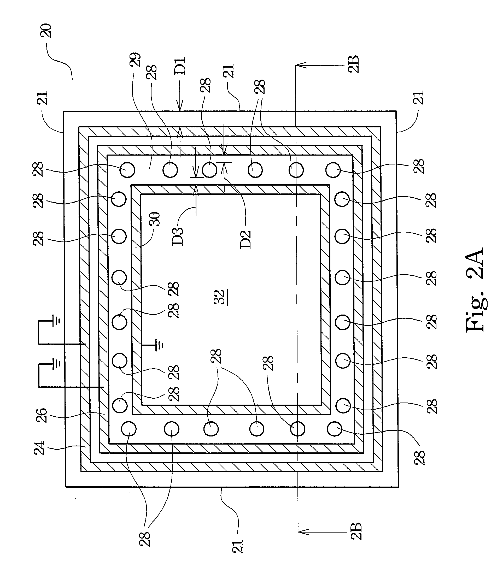
[0020]FIG. 2A illustrates a top view of a first embodiment of the present invention, which includes semiconductor chip (also referred to as die in the packaging art) 20. Seal rings 24 and 26 are formed close to edges 21 of chip 20. Seal rings 24 and 26 are preferably grounded. As is known in the art, seal ring 26 is sometimes referred to as a main seal ring, while seal ring 24 is referred to as a sacrificial seal ring. Sacrificial seal ring 24 is optional.

[0021]Through-silicon vias 28 are formed in an inner region encircled by seal ring 26. In an embodiment, TSVs 28 are locat...


PUM


Abstract

A semiconductor chip includes a through-silicon via (TSV), a device region, and a cross-talk prevention ring encircling one of the device region and the TSV. The TSV is isolated from substantially all device regions comprising active devices by the cross-talk prevention ring.

Description

TECHNICAL FIELD[0001]This invention relates generally to integrated circuits, and more particularly to structures and methods for reducing the cross-talks between through-silicon vias and integrated circuits in semiconductor chips.BACKGROUND[0002]Since the invention of integrated circuits, the semiconductor industry has experienced continuous rapid growth due to constant improvements in the integration density of various electronic components (i.e., transistors, diodes, resistors, capacitors, etc.). For the most part, this improvement in integration density has come from repeated reductions in minimum feature size, allowing more components to be integrated into a given chip area.[0003]These integration improvements are essentially two-dimensional (2D) in nature, in that the volume occupied by the integrated components is essentially on the surface of the semiconductor wafer. Although dramatic improvements in lithography have resulted in considerable improvements in 2D integrated cir...

Claims


Application Information

Patent Timeline
IPC IPC(8): H01L23/552
CPCH01L23/481H01L23/552H01L23/562H01L23/585H01L2224/16H01L25/0657H01L2223/6688H01L2225/06513H01L2225/06541H01L23/66
Inventor KUO, CHEN-CHENG
Owner TAIWAN SEMICON MFG CO LTD
Why Eureka
Try Eureka