

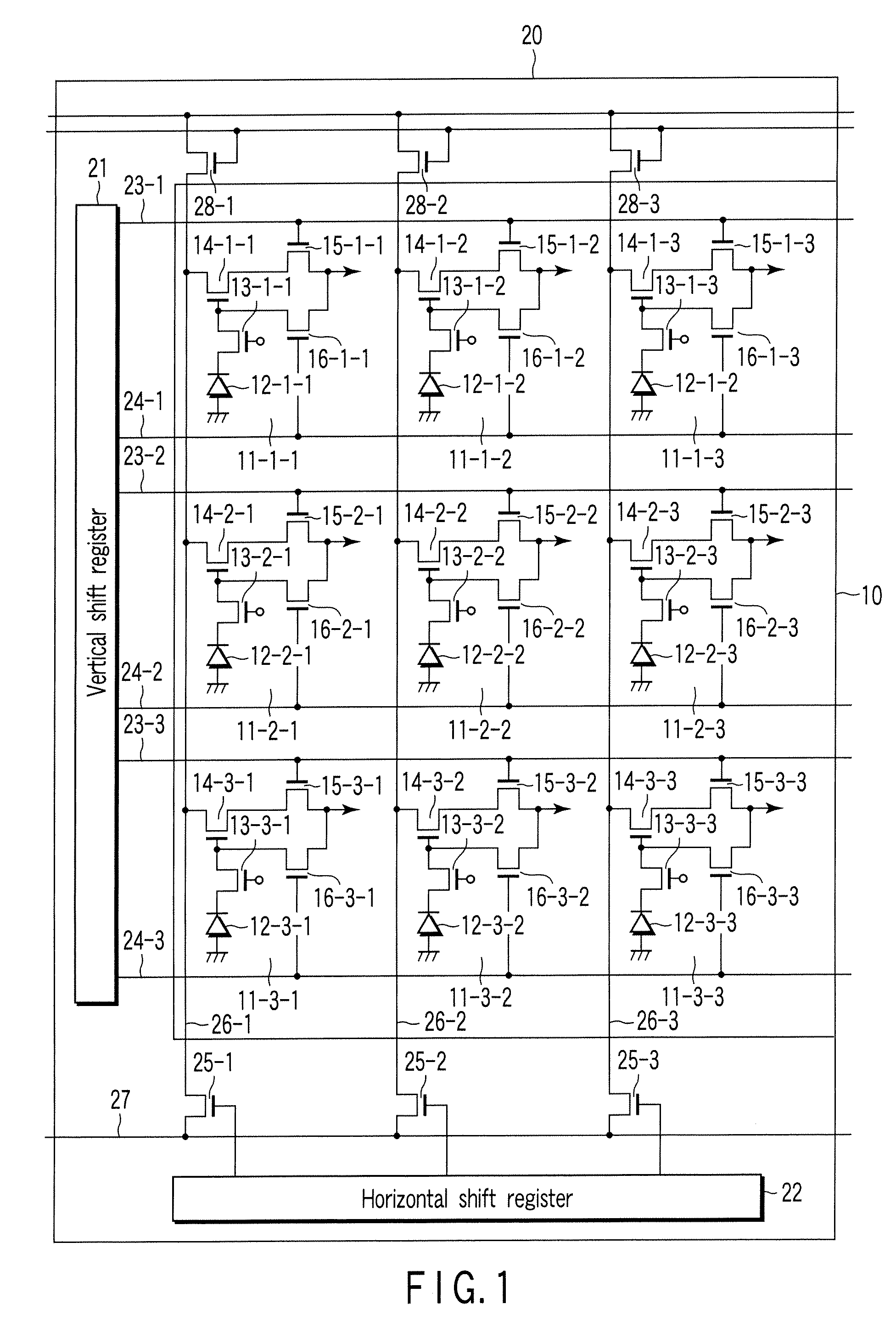
Solid-state imaging device
a solid-state imaging and imaging device technology, applied in the direction of color television, television system, radio control device, etc., can solve the problems of variation in dark-time level, inability to use the n-type substrate, vertical over-draining structure,
- Summary
- Abstract
- Description
- Claims
- Application Information
AI Technical Summary
Benefits of technology
Problems solved by technology
Method used
Image

Examples
first embodiment
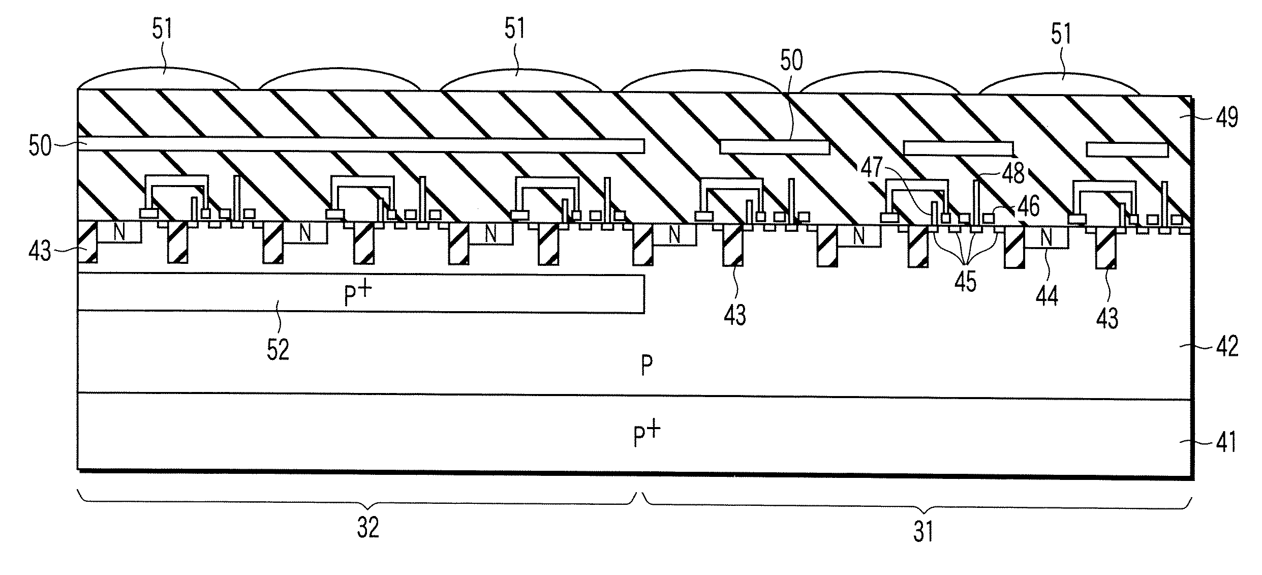
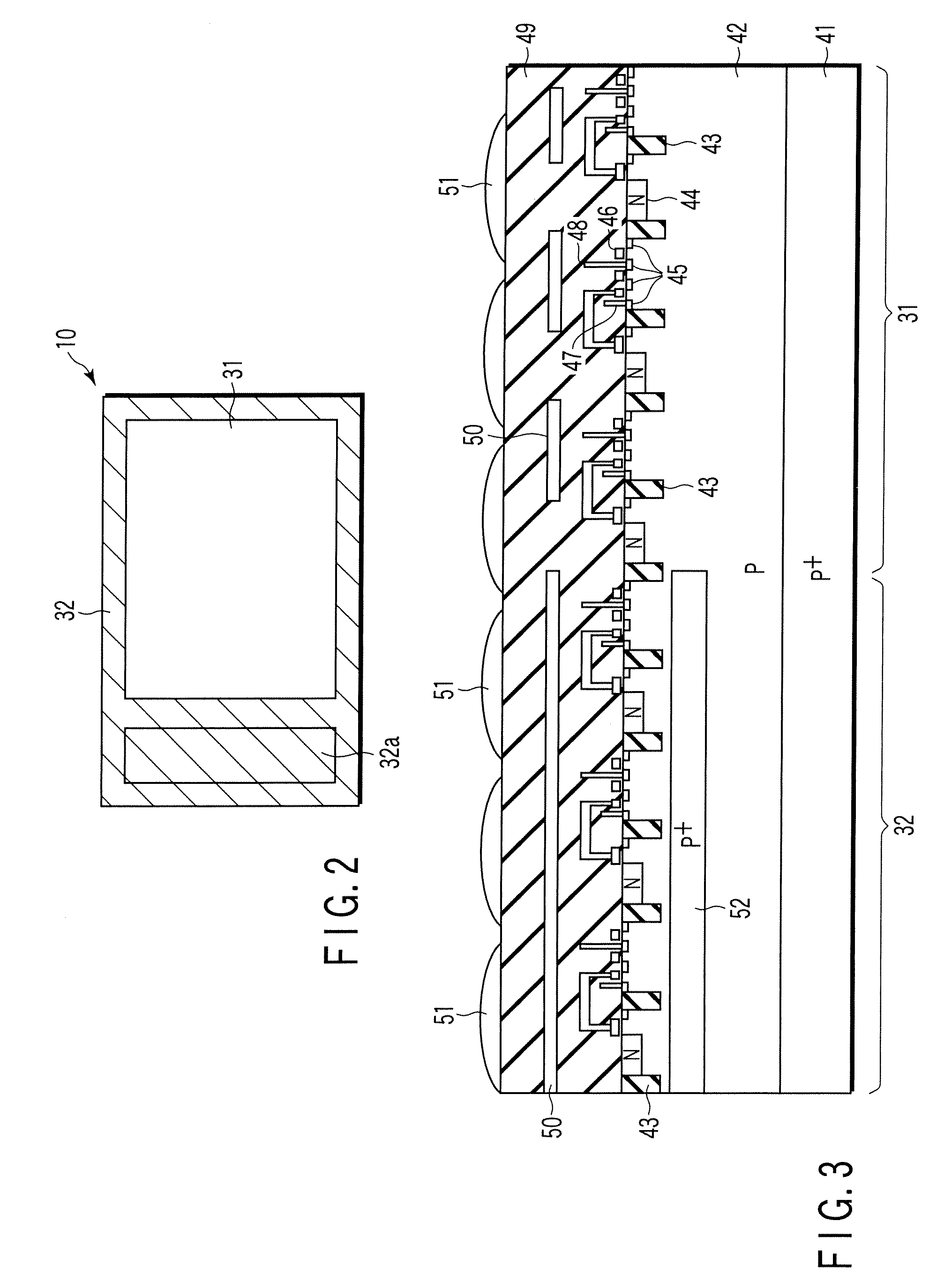
[0028]FIG. 3 is a cross-sectional view of an amplification-type MOS image sensor according to a first embodiment of the invention. FIG. 3 shows, for example, parts of the imaging region 31 and OB pixel region 32 shown in FIG. 2.
[0029]A P-type silicon substrate 42 is formed on a P+-type silicon substrate 41 having a relatively high P-type impurity concentration. The P-type impurity concentration in the P-type silicon substrate 42 is lower than that in the P+-type silicon substrate 41. The P+-type silicon substrate 41 and P-type silicon substrate 42 constitute a PonP+-type silicon substrate. The PonP+-type silicon substrate has a characteristic function of collecting signal carriers, which have been photoelectrically converted within the substrate, in the low-concentration P-type silicon substrate 42. Device isolation regions 43, which isolate the unit pixel regions and OB pixel regions, are formed in a surface region of the P-type silicon substrate 42. A photoelectric conversion regi...
second embodiment
[0033]FIG. 4 is a cross-sectional view of an amplification-type MOS image sensor according to a second embodiment of the invention. FIG. 4 shows, for example, parts of the imaging region 31 and OB pixel region 32 shown in FIG. 2. Although not shown in FIG. 2, the OB pixel region 32 includes a dummy OB pixel region 32b for obtaining a reference signal, in addition to the effective OB pixel region 32a. The dummy OB pixel region 32b includes a plurality of dummy optical black pixels.
[0034]In the amplification-type MOS image sensor shown in FIG. 4, like the image sensor shown in FIG. 3, a P+-type barrier layer 52 is formed in the P-type silicon substrate 42 under the OB pixel region 32. The P+-type barrier layer 52 is of the same conductivity type as the P-type silicon substrate 42 and has an impurity concentration higher than the impurity concentration of the P-type silicon substrate 42. In this case, the P+-type barrier layer 52, which is of the same conductivity type as the P-type si...
third embodiment
[0038]FIG. 5 is a cross-sectional view of an amplification-type MOS image sensor according to a third embodiment of the invention. FIG. 5 shows, for example, parts of the imaging region 31 and OB pixel region 32 shown in FIG. 2. The image sensor shown in FIG. 5 is similar to that shown in FIG. 4 in that the P+-type barrier layer 52 is formed so as to surround the OB pixel region 32 in the planar fashion, but they differ in that no dummy OB pixel is formed in the region of the P+-type barrier layer 52 in the image sensor shown in FIG. 5.
[0039]According to the amplification-type MOS image sensor shown in FIG. 5, the same advantageous effect as with the amplification-type MOS image sensor shown in FIG. 4 can be obtained. Moreover, the size of the P+-type barrier layer 52 can be reduced regardless of the size of the dummy OB pixel. Thereby, the size of the P+-type barrier layer 52 can be set by a factor different from such a factor as reduction in chip size.
PUM
 Abstract
Description
Claims
Application Information