

Solid-state imaging device, camera module and electronic equipment module
a technology of solid-state imaging and camera modules, applied in the direction of color television, radio control devices, television systems, etc., can solve the problems of increasing the number of production processes, increasing the cost, and deteriorating the yield ra
- Summary
- Abstract
- Description
- Claims
- Application Information
AI Technical Summary
Benefits of technology
Problems solved by technology
Method used
Image

Examples
first embodiment
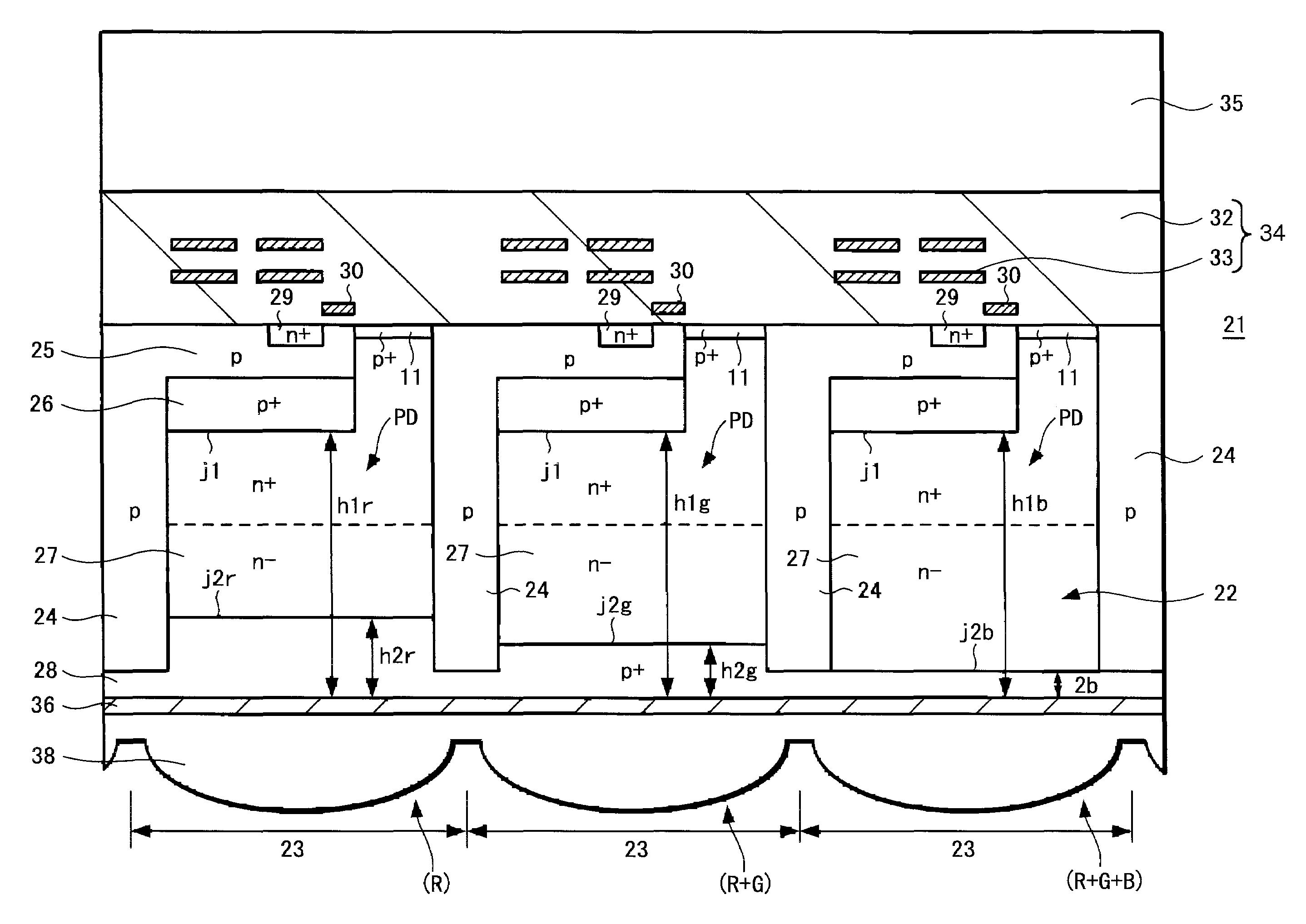
[0023]FIG. 1 shows a first embodiment in which a back-illuminated type solid-state imaging device according to the present invention is applied to a CMOS solid-state imaging device. The figure shows a pixel portion in an imaging region.
[0024]A back-illuminated type CMOS solid-state imaging device 21 according to the present embodiment, pixel-isolation regions 24 made of p type, that is a second conductive type, semiconductor regions are formed in a first conductive type, for example n-type, silicon semiconductor substrate 22 to separate unit pixel regions 23 from each other, and a photodiode PD which serves as a photoelectric conversion element and a required number of MOS transistors Tr for reading out signal charges obtained through photoelectric conversion and accumulated in the photodiode PD are formed within each of the pixel regions 23 surrounded by the p-type pixel-isolation regions 24.
[0025]The p-type pixel-isolation regions 24 are formed in the direction of the depth of the...
second embodiment
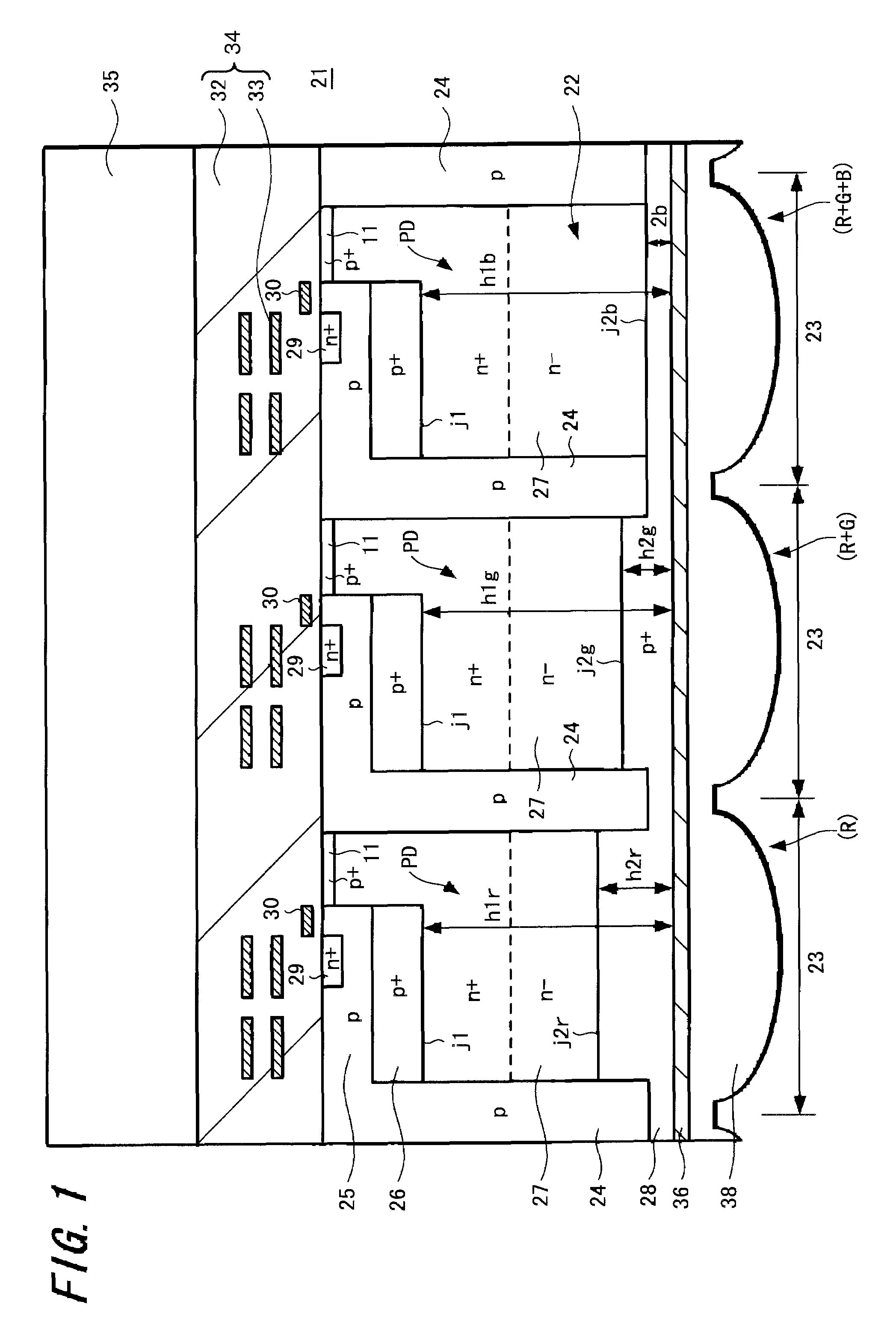
[0034]FIG. 2 shows a second embodiment in which a back-illuminated type solid-state imaging device according to the present invention is applied to a CMOS solid-state imaging device. The figure shows a pixel portion in an imaging region, similarly to the above described embodiment.
[0035]In a back-illuminated type CMOS solid-state imaging device 41 according to the present embodiment, a color filter is omitted, and only light of a specific wavelength or shorter is photoelectrically converted in photodiodes PD by adjusting junction depths h1 [h1 r, h1 g, h1 b] from the back surface of pn junctions j1 [j1 r, j1 g, j1 b] on the front surface side of the substrate on which photodiodes PD of pixels are formed. Specifically, in the present embodiment, the pn junction depth (that is, the position in the direction of depth) h1 r corresponding to a red pixel is made greater than the other pn junction depths corresponding to green and blue pixels, the pn junction depth h1 b corresponding to a ...
third embodiment
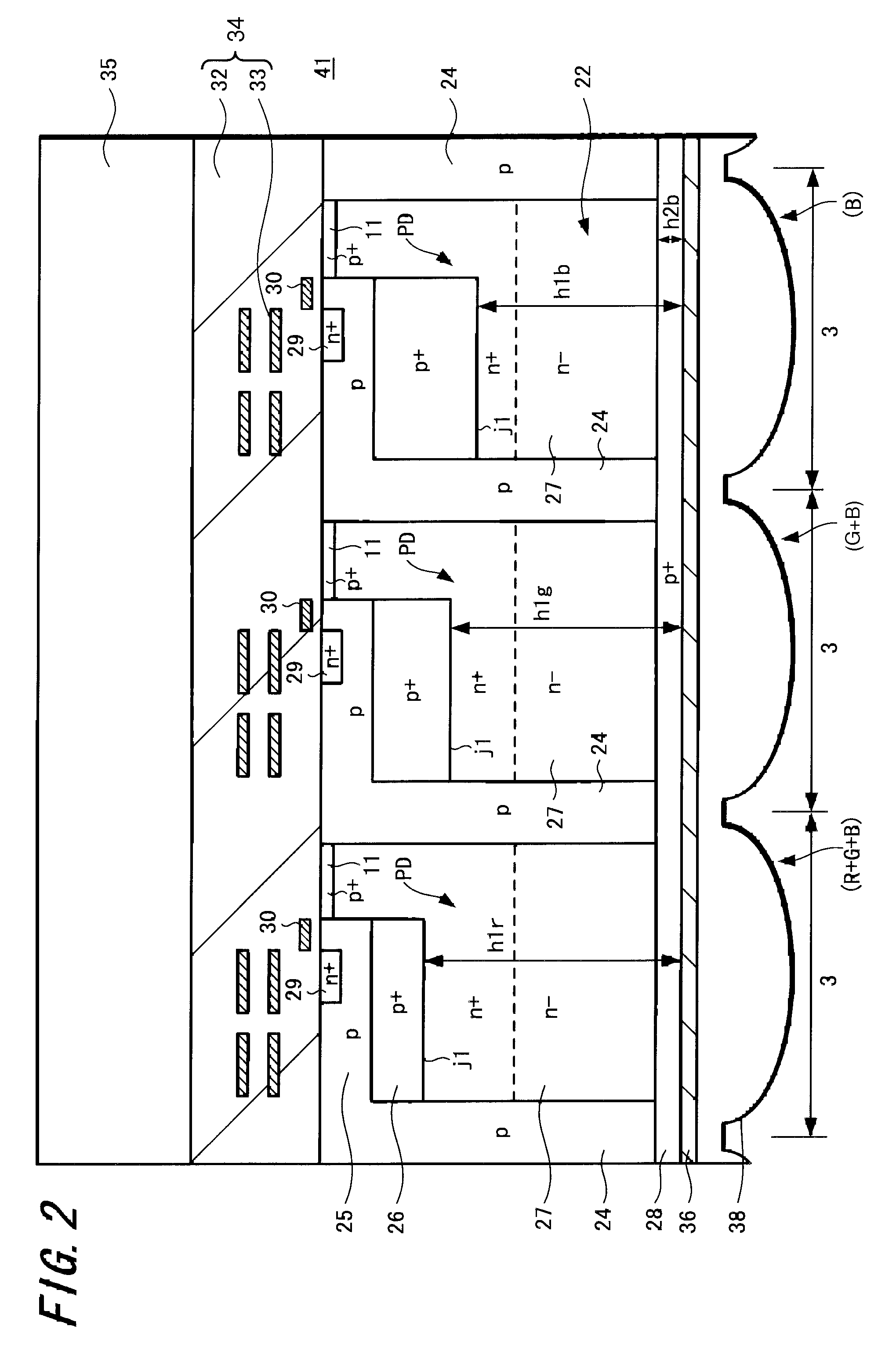
[0041]FIG. 3 shows a third embodiment in which a back-illuminated type solid-state imaging device according to the present invention is applied to a CMOS solid-state imaging device. The figure shows a pixel portion in an imaging region, similarly to the above described embodiments.
[0042]In a back-illuminated type CMOS solid-state imaging device 51 according to the present embodiment, a color filter is omitted, and only light in a specific wavelength range is photoelectrically converted in photodiodes PD by combining the junction depths h2 [h2 r, h2 g, h2 b] in FIG. 1 that are the depths from the back surface, of the pn junctions j2 [j2 r, j2 g, j2 b] and the junction depths h1 [h1 r, h1 g, h1 b] in FIG. 2 that are the depths from the back surface, of the pn junctions j1 [j1 r, j1 g, j1 b], and by adjusting the regions of photodiodes PD between the junction depths h2 and the junction depths h1, that is, the positions in the direction of depth of n-type semiconductor regions 27.
[0043]...
PUM
 Abstract
Description
Claims
Application Information