MOS devices with partial stressor channel

a technology of stressors and mos, applied in the direction of semiconductor devices, semiconductor/solid-state device details, electrical apparatus, etc., can solve the problems of conventional methods for improving the performance of metal-oxide-semiconductors, mos, has run into bottlenecks, and conventional stressor formation processes suffer drawbacks, etc., to reduce the probability of punching through and increase the stress in the channel region

Active Publication Date: 2009-06-30
TAIWAN SEMICON MFG CO LTD
View PDF8 Cites 44 Cited by
  • Summary
  • Abstract
  • Description
  • Claims
  • Application Information

AI Technical Summary

Benefits of technology

[0012]The advantageous features of the present invention include reduced probability of punch-through and increased stress in the channel region.

Problems solved by technology

With the continuous scaling of integrated circuits, the conventional methods for improving performance of metal-oxide-semiconductor (MOS) devices, such as shortening gate lengths of MOS devices, has run into bottlenecks.
The conventional stressor formation processes suffer drawbacks, however. FIG. 1 illustrates a conventional MOS device.
However, the decrease in distance D may result in a punch-through between source and drain regions, and a leakage current may flow between source and drain regions in path 8 below the channel region.
This problem is further worsened due to the scaling down of integrated circuits, which causes distance D to further decrease.

Method used


Image

  • MOS devices with partial stressor channel
  • MOS devices with partial stressor channel
  • MOS devices with partial stressor channel

Examples


Embodiment Construction

[0016]The making and using of the presently preferred embodiments are discussed in detail below. It should be appreciated, however, that the present invention provides many applicable inventive concepts that can be embodied in a wide variety of specific contexts. The specific embodiments discussed are merely illustrative of specific ways to make and use the invention, and do not limit the scope of the invention.

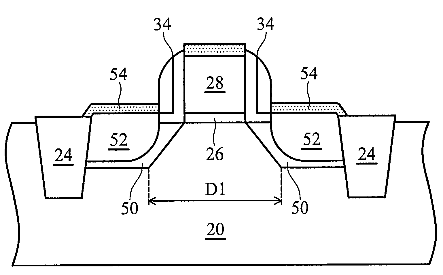
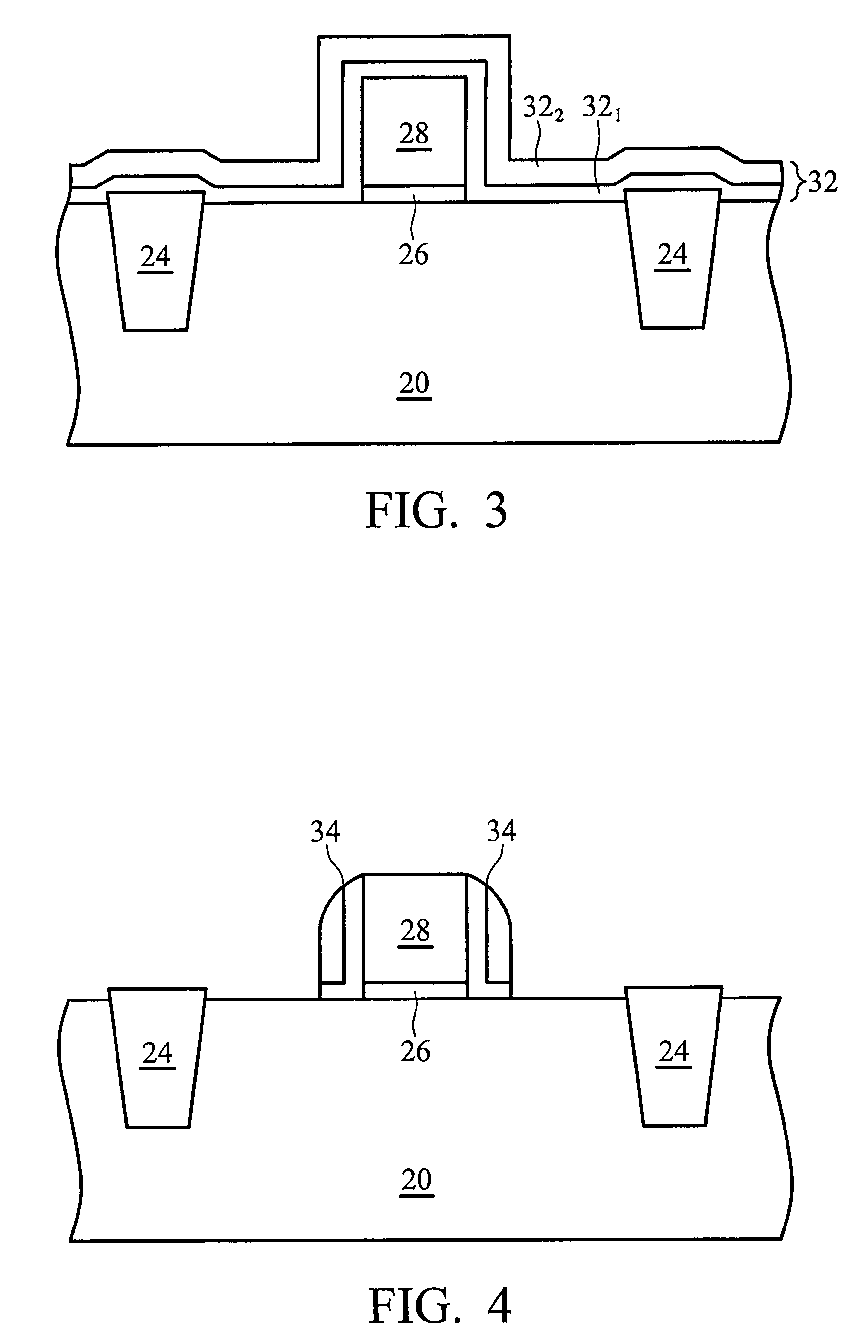
[0017]A novel method for forming MOS devices having channel stressors is provided. The intermediate stages of manufacturing embodiments of the present invention are illustrated in FIGS. 2 through 11. Throughout the various views and illustrative embodiments of the present invention, like reference numbers are used to designate like elements.

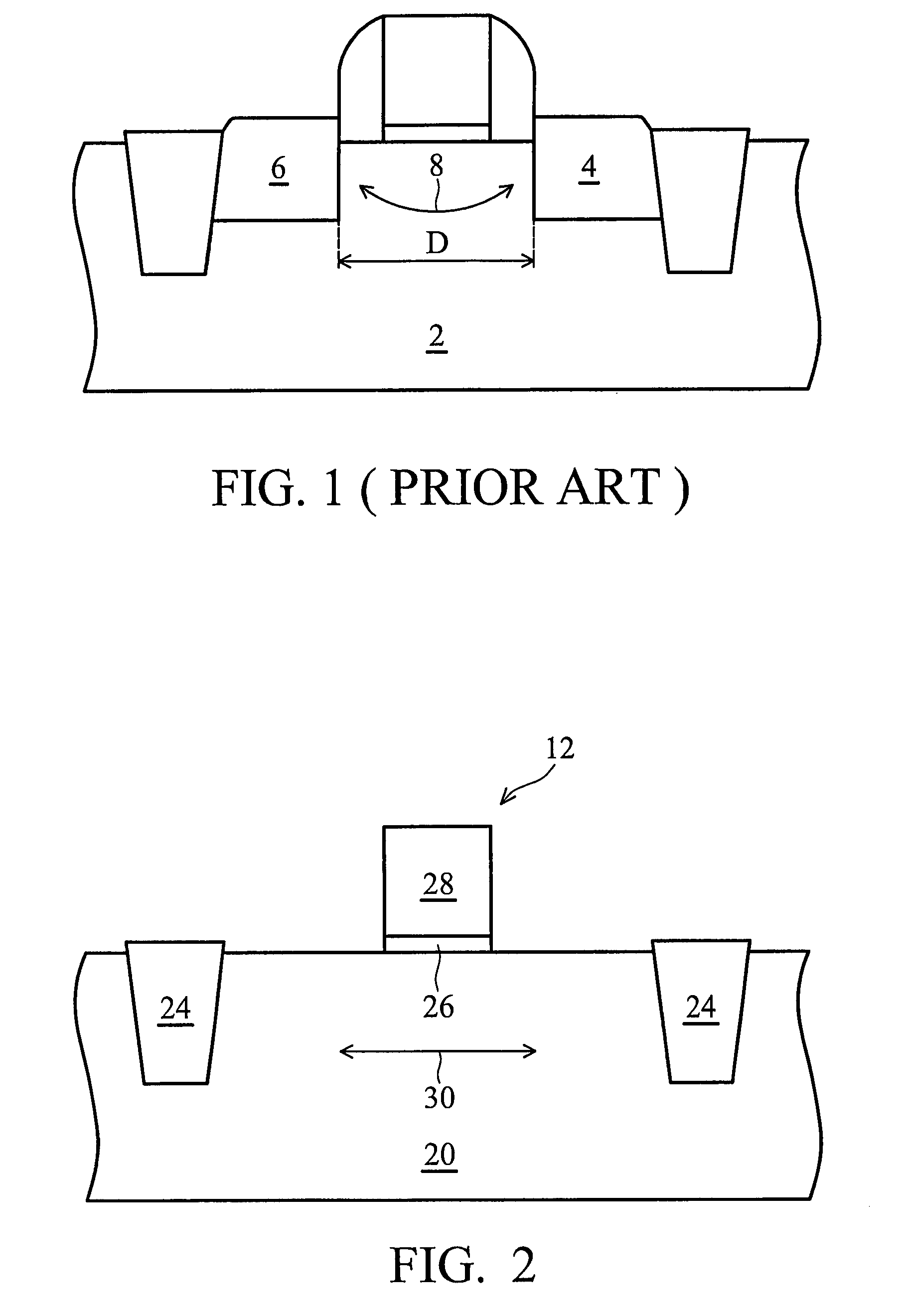
[0018]FIG. 2 illustrates a substrate 20. Preferably, substrate 20 comprises bulk silicon. Alternatively, substrate 20 comprises bulk SiGe or other semiconductor materials. Substrate 20 may also have a composite structure such as silicon-on...


PUM


Abstract

A semiconductor structure includes a semiconductor substrate having a first lattice constant; a gate dielectric on the semiconductor substrate; a gate electrode on the semiconductor substrate; and a stressor having at least a portion in the semiconductor substrate and adjacent the gate electrode. The stressor has a tilted sidewall on a side adjacent the gate electrode. The stressor includes a first stressor layer having a second lattice constant substantially different from the first lattice constant; and a second stressor layer on the first stressor layer, wherein the second stressor has a third lattice constant substantially different from the first and the second lattice constants.

Description

CROSS REFERENCES[0001]This application relates to and claims the benefit of U.S. Provisional patent application Ser. No. 60 / 844,786, filed Sep. 15, 2006, entitled “MOS Devices with Partial Stressor Channel,” which patent application is incorporated herein by reference.TECHNICAL FIELD[0002]This invention relates generally to integrated circuits, and more particularly to structure and formation methods of MOS devices with channel stressors.BACKGROUND[0003]Reductions in sizes and inherent features of semiconductor devices have enabled continued improvements in speed, performance, density, and cost per unit function of integrated circuits over the past few decades. With the continuous scaling of integrated circuits, the conventional methods for improving performance of metal-oxide-semiconductor (MOS) devices, such as shortening gate lengths of MOS devices, has run into bottlenecks. To further enhance the performance of MOS devices, stress may be introduced in the channels of the MOS dev...

Claims


Application Information

Patent Timeline
Patent Type & Authority Patents(United States)
IPC IPC(8): H01L29/06
CPCH01L29/045H01L29/6659H01L29/66628H01L29/66636H01L29/7833H01L29/7836H01L29/7848H01L29/165H01L29/665H01L29/6656Y10S438/938
Inventor YU, MING-HUALIANG, MONG-SONGLEE, TZE-LIANGLI, JR-HUNG
Owner TAIWAN SEMICON MFG CO LTD
Why Eureka
Try Eureka