Display device

a display device and display technology, applied in the field of self-light-emitting display devices, can solve the problems of inferior viewing angle characteristics, difficult material selection, interference of light reflected on the interface between each layer, etc., and achieve the effects of improving viewing angle characteristics, simple structure, and improving viewing angle characteristics

Inactive Publication Date: 2009-06-30
SEMICON ENERGY LAB CO LTD
View PDF16 Cites 41 Cited by
  • Summary
  • Abstract
  • Description
  • Claims
  • Application Information

AI Technical Summary

Benefits of technology

[0016]In view of the foregoing, it is a primary object of the invention to provide an active matrix display device which can easily improve the viewing angle characteristics.
[0027]The display device of the invention is a display device having the improved viewing angle characteristics with a simple structure. Since the display device of the invention has the improved viewing angle characteristics, favorable image display can be provided. In addition, the display device of the invention can be manufactured without the need for additional steps or materials, thus a display device with the improved viewing angle characteristics can be provided easily.

Problems solved by technology

When light travels through the stacked insulating films, there might be a case where light reflected on the interface between each layer interferes with each other (called multiple interference) due to the difference in refraction factor of each insulating film.
As a result, emission spectrum changes dependently on the angle seen from the emission side, leading to the inferior viewing angle characteristics.
However, in the structure of Patent Document 1, it is quite difficult to select materials which can satisfy both the desired refraction factor and the function of each layer such as an insulating property and a passivation property since the refraction factor is an intrinsic value to each material.
Therefore, there is a possibility that the degradation of the viewing angle characteristics cannot be sufficiently suppressed in a light-emitting device such as an active matrix light-emitting device where light is emitted outside through a plurality of layers in addition to the light-emitting element.

Method used


Image

  • Display device
  • Display device
  • Display device

Examples


embodiment mode 1

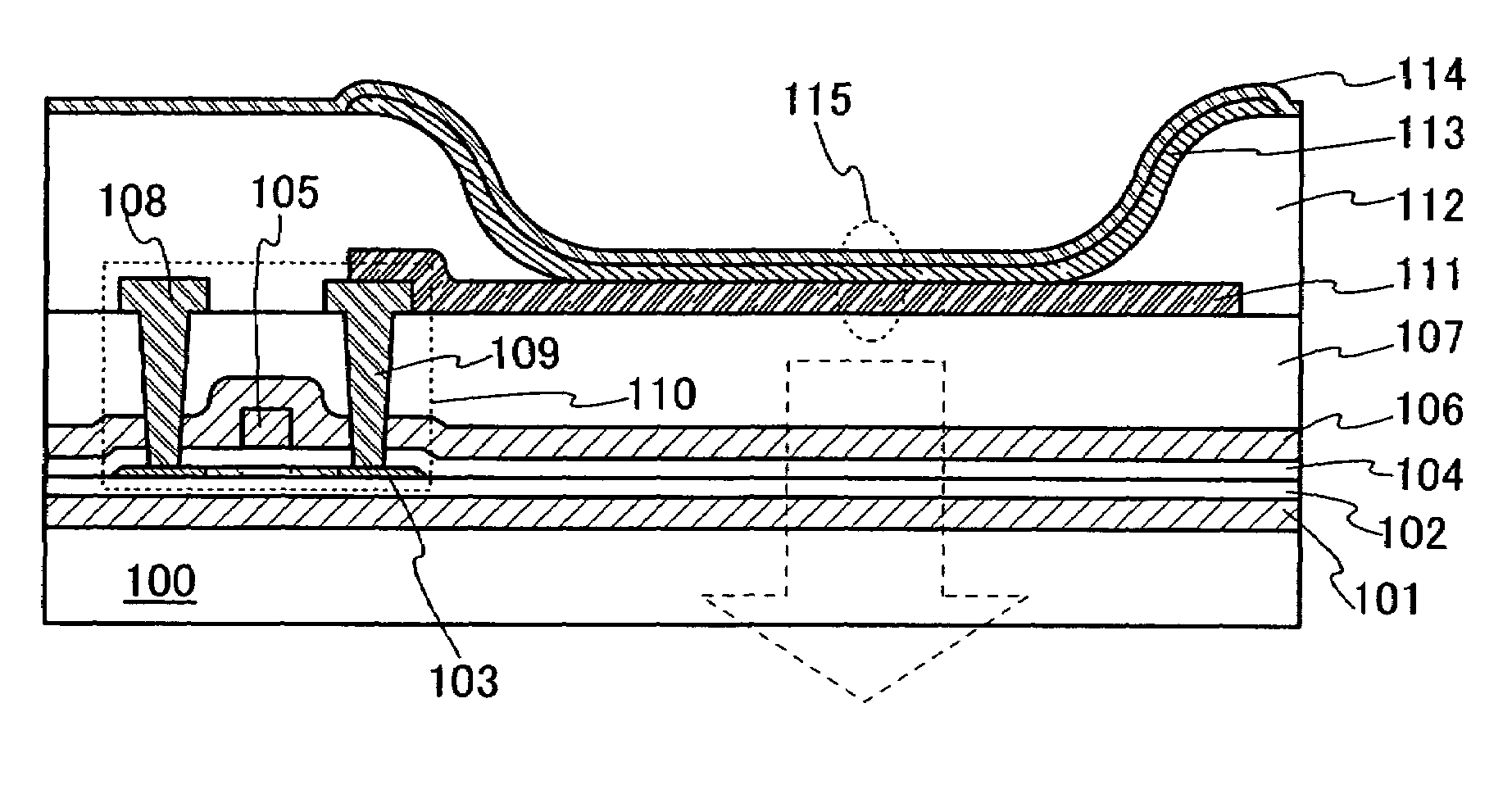
[0057]In this embodiment, description is made with reference to FIG. 1 on an example of a display device of the invention.

[0058]In the display device in this embodiment mode, a first base insulating film 101 and a second base insulating film 102 are formed in this order over a light-transmissive substrate 100. On the second base insulating film 102, a semiconductor layer 103 is formed, and a gate insulating film 104 is formed covering the semiconductor layer 103 and the second base insulating film 102. On the gate insulating film 104, a gate electrode 105 is formed in a partially overlapped manner with the semiconductor layer 103. The gate electrode 105 and the gate insulating film 104 are covered with a first insulating film 106, and the first insulating film 106 is covered with a second insulating film 107. On the second insulating film 107, electrodes 108 and 109 are provided to be electrically connected to the semiconductor layer 103 through contact holes which are formed to pen...

embodiment mode 2

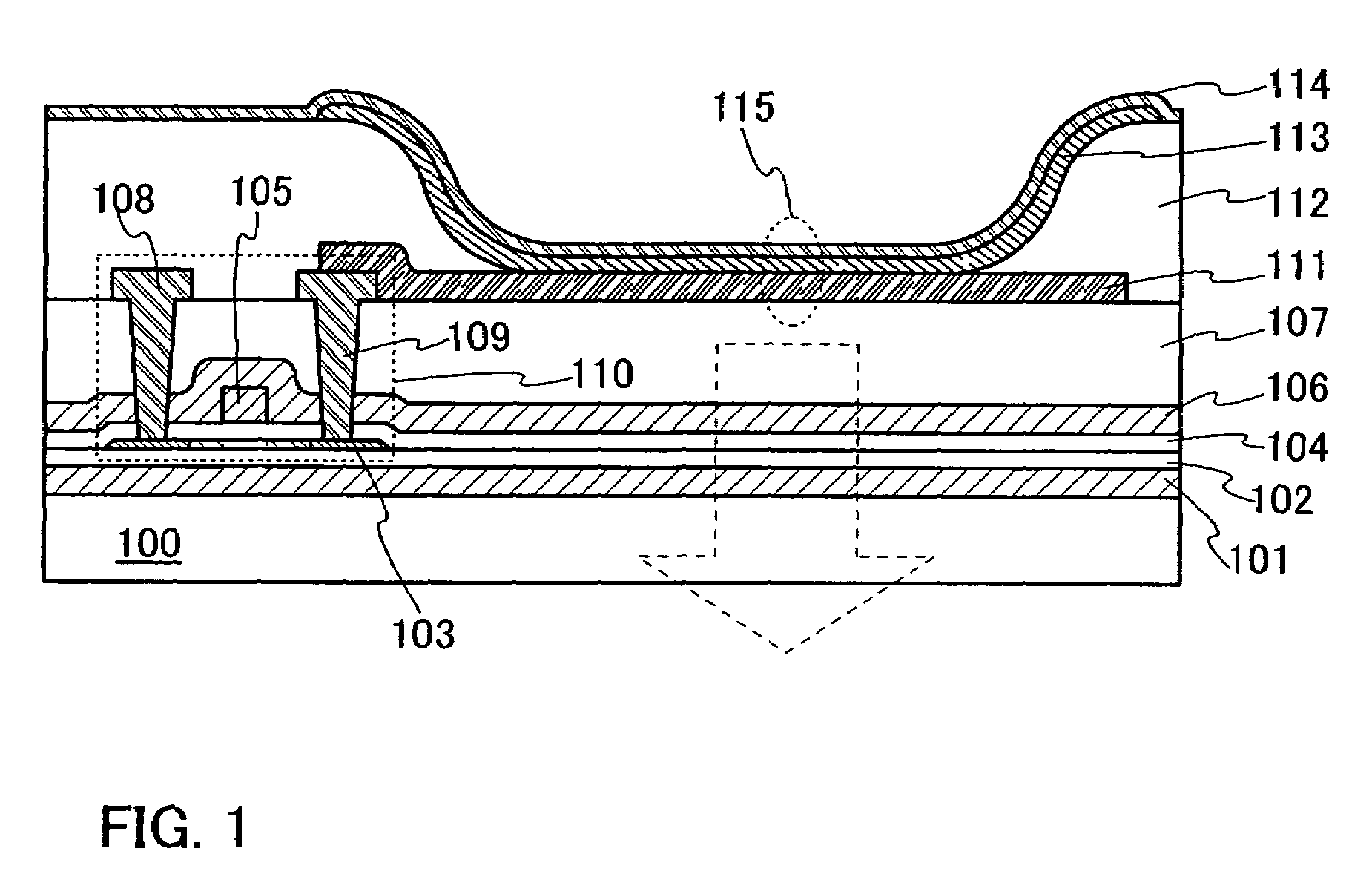
[0085]In this embodiment mode, description is made with reference to FIG. 2 on another structure of the invention. The display device in this embodiment mode has substantially the same structure as the display device in Embodiment Mode 1; however, the first insulating film 106 in Embodiment Mode 1 is not provided. In this case, only the first base insulating film 101 has a different refraction factor from other films, among the layers through which the light emitted from the light-emitting element 115 travels to the outside.

[0086]Therefore, by setting the optical thickness L of the first base insulating film 101 to be substantially equal to the integral multiple of λ / 2 on the assumption that the center wavelength of the light emitted from the light-emitting element 115 is λ, the light reflected on the incident interface of the film can be attenuated by the light reflected on the emission interface of the film, thus the reflected light generated by such film can be drastically decrea...

embodiment mode 3

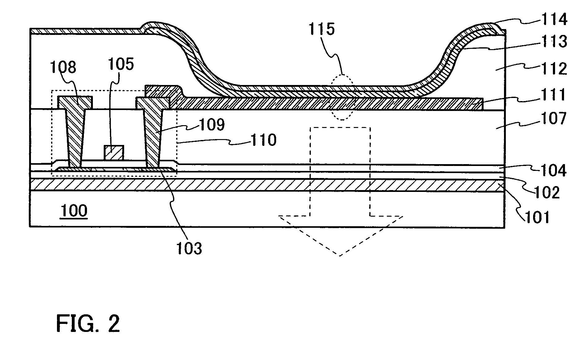
[0090]In this embodiment mode, description is made with reference to FIG. 3 on still another structure of the invention. The display device in this embodiment mode has substantially the same structure as the display device in Embodiment Mode 1; however, the second base insulating film 102 in Embodiment Mode 1 is not provided and only the base insulating film 116 is provided as a base insulating film. This embodiment mode illustrates an example in which the base insulating film 116 is formed of silicon nitride containing oxygen. In this case, two layers which are the first insulating film 106 and the base insulating film 116 have different refraction factors from other films, among the layers through which the light emitted from the light-emitting element 115 travels to the outside.

[0091]Here, by setting each optical thickness L of the first insulating film 106 and the base insulating film 116 to be substantially equal to the integral multiple of λ / 2 on the assumption that the center...


PUM


Abstract

An active matrix display device which can easily improve the viewing angle characteristics. In the active matrix display device where light is emitted in the direction of a substrate over which thin film transistors are formed, when focusing on the multiple interference caused by the light emitted from a light-emitting element, which is reflected on the film used for forming the thin film transistors, effect on the multiple interference can be drastically reduced by forming the reflecting film to have the substantial optical thickness of λ / 2, without losing the function of the thin film transistor.

Description

BACKGROUND OF THE INVENTION[0001]1. Field of the Invention[0002]The present invention relates to a display device, and more particularly to a self-light-emitting display device having the improved viewing angle characteristics.[0003]2. Description of the Related Art[0004]A light-emitting device which uses light emission from electroluminescence elements (light-emitting elements) has been attracting attention as a display device with a wide viewing angle and low power consumption.[0005]As a driving method of the light-emitting device which is mainly used for image display, there are an active matrix driving method and a passive matrix driving method. As for the light-emitting device using the active matrix driving method, emission / non-emission or the like of a light-emitting element can be controlled in each pixel. Therefore; it can be driven with lower power consumption than the passive matrix light-emitting device. Thus, the light-emitting device can be suitably mounted as a displa...

Claims


Application Information

Patent Timeline
Patent Type & Authority Patents(United States)
IPC IPC(8): H01J1/62H01J63/04H01L27/32H01L51/52H05B33/22
CPCH01L51/5262H01L27/3244H10K59/12H10K50/85
Inventor GODO, HIROMICHIMATSUBARA, TOMOESAKAKURA, MASAYUKI
Owner SEMICON ENERGY LAB CO LTD
Why Eureka
Try Eureka