Method of controlling the resistance in a variable resistive element and non-volatile semiconductor memory device

a technology of variable resistive elements and memory devices, which is applied in the direction of information storage, static storage, digital storage, etc., can solve the problems of power consumption of memory devices that is most likely to be increased, the logic circuit of conducting logic functions may be predominant in power consumption, and the primary function of such mobile devices including the life of batteries and the speed of access to data remain not high enough to be satisfied, so as to reduce the application time of program voltage pulses, increase the stability of monopolar switching action, and minimize the effect of program voltage puls

Inactive Publication Date: 2009-07-07
DENSO CORP
View PDF4 Cites 58 Cited by
  • Summary
  • Abstract
  • Description
  • Claims
  • Application Information

AI Technical Summary

Benefits of technology

[0033]Accordingly, the method of controlling the resistance of a variable resistive element of the first feature allows the variable resistive element to be shifted from the initial resistive characteristic after the production to the variable resistance state capable of the mono-polar switching action in the forming step, hence making the mono-polar switching action stable and consistent.
[0042]According to the non-volatile semiconductor memory device of the fourth feature, since the diode has a current rectifying property, the leak current specific to a cross-point type memory cell array can be decreased and the stableness of the memory actions can be ensured, when the memory cells are arranged in a cross-point type memory cell array. In particular, even if the memory cell is arranged to flow its current in one direction, its variable resistive element is capable of conducting the mono-polar switching action thus ensuring the program action and the erase action.

Problems solved by technology

However, the primary functions of such mobile devices including the life of batteries and the speed of access to data remain not high enough to be satisfied and will hence be demanded for much improvement.
When such a mobile device is active in motion, its logic circuit for conducting logic functions may be predominant in the power consumption.
In a standby mode, the power consumption of a memory device may be increased most.
It is not negligible that the power consumption at the standby mode disturbs the lengthening of the life of batteries in a mobile device.
However, there is no satisfactory solution over the relationship between the condition for applying the forming voltage pulse to shift from the initial state to the variable resistance state for enabling the mono-polar switching action and the resistant property in the variable resistance state.

Method used


Image

  • Method of controlling the resistance in a variable resistive element and non-volatile semiconductor memory device
  • Method of controlling the resistance in a variable resistive element and non-volatile semiconductor memory device
  • Method of controlling the resistance in a variable resistive element and non-volatile semiconductor memory device

Examples


Embodiment Construction

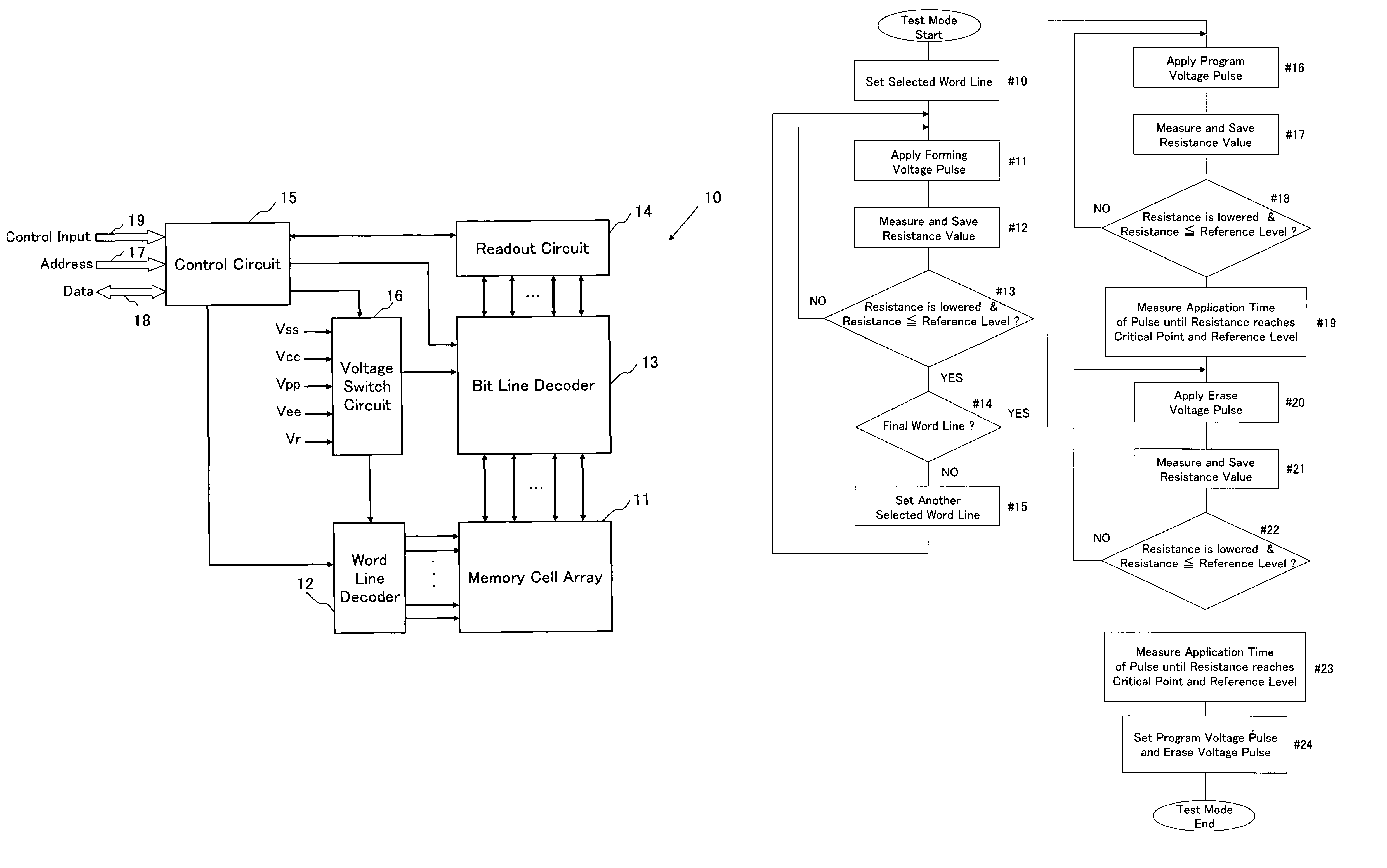
[0067]A non-volatile semiconductor memory device according to the present invention (thus referred to as an inventive device hereinafter) and a method of controlling the resistance in a variable resistive element in the inventive device (referred to as an inventive method hereinafter) will be described referring to the relevant drawings.

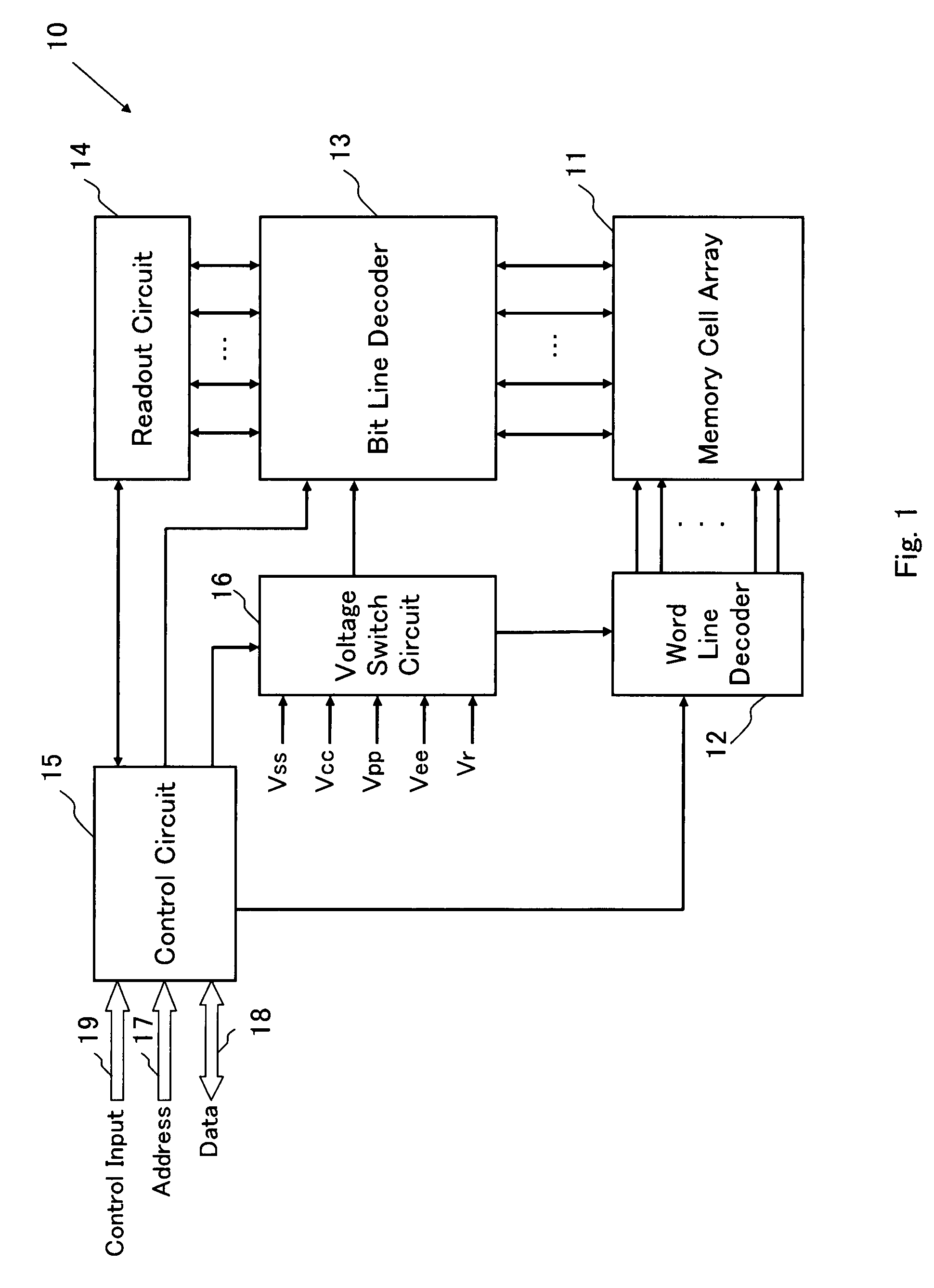
[0068]FIG. 1 illustrates a block diagram of one embodiment of the inventive device 10. As shown in FIG. 1, the inventive device 10 comprises an array of memory cells 11, a word line decoder 12, a bit line decoder 13, a readout circuit 14, a control circuit 15, and a voltage switch circuit 16.

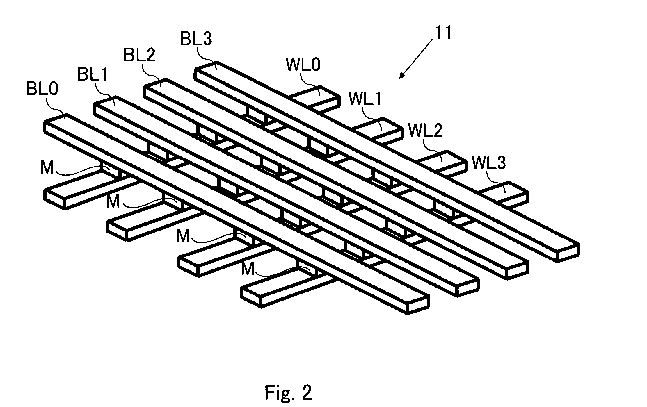
[0069]The memory cell array 11 includes a number of non-volatile memory cells arranged in rows and columns, each memory cell determined by an address input from the outside is electrically programmed with a data. The data can be readout from the memory cell determined by the address input. More particularly, in response to an address signal received from an addre...


PUM


Abstract

The method of controlling a resistance of a variable resistive element comprises a forming step for shifting the variable resistive element from an initial state after the production to a variable resistance state capable of a stable mono-polar switching action where a variable resistive characteristic of the variable resistive element is turned to a program resistive characteristic by applying a program voltage pulse to the variable resistive element for first pulse application time and to an erase resistive characteristic by applying an erase voltage pulse equal in polarity to the program voltage pulse to the variable resistive element for second pulse application time longer than the first pulse application time, wherein one or more forming voltage pulses equal in polarity to the program voltage pulse is applied to the variable resistive element for third pulse application time longer than the second pulse application time.

Description

CROSS REFERENCE TO RELATED APPLICATION[0001]This Nonprovisional application claims priority under 35 U.S.C. §119(a) on Patent Application No. 2006-046234 filed in Japan on Feb. 23, 2006, the entire contents of which are hereby incorporated by reference.BACKGROUND OF THE INVENTION[0002]1. Field of the Invention[0003]The present invention relates to a non-volatile semiconductor memory device having an array of variable resistive elements of two-port structure type and particularly to a resistance controlling method of applying a voltage pulse to the two ports of a variable resistive element of interest to change the resistance characteristic of the variable resistive element.[0004]2. Description of the Related Art[0005]There will be an epoch where desired data can be obtained and kept at any time and any location. As mobile devices such as mobile telephones or PDAs (portable, personal data communication devices) have been spread in the market, they allow various data to be accessed wi...

Claims


Application Information

Patent Timeline
Patent Type & Authority Patents(United States)
IPC IPC(8): G11C11/00
CPCG11C11/16G11C11/5685G11C13/0007G11C13/0069G11C29/50008G11C29/50G11C2013/0083G11C2013/009G11C2213/31G11C2013/0092
Inventor MORIMOTO, HIDENORI
Owner DENSO CORP
Why Eureka
Try Eureka