Method and apparatus for measuring the curvature of reflective surfaces

a curvature and reflective surface technology, applied in the direction of measuring devices, instruments, using optical means, etc., can solve the problems of inability to measure the curvature of a fast-moving wafer, the apparatus is relatively delicate and expensive, and the system proposed heretofore is not well suited to monitoring the strain during wafer growth under typical production conditions

Active Publication Date: 2009-08-04
VEECO INSTR
View PDF14 Cites 35 Cited by
  • Summary
  • Abstract
  • Description
  • Claims
  • Application Information

AI Technical Summary

Problems solved by technology

However, the systems proposed heretofore have not been well suited to monitoring strain during wafer growth under typical production conditions.
This apparatus is relatively delicate and expensive, and is typically incapable of measuring the curvature of a fast-moving wafer.
Devices of this type also require a large diameter view port, which further limits their use with industrial MOCVD reactors.
However, instruments of this type require precise placement and movement of the wafer, and are not well suited for measure wafer curvature in a production environment.

Method used


Image

  • Method and apparatus for measuring the curvature of reflective surfaces
  • Method and apparatus for measuring the curvature of reflective surfaces
  • Method and apparatus for measuring the curvature of reflective surfaces

Examples


Embodiment Construction

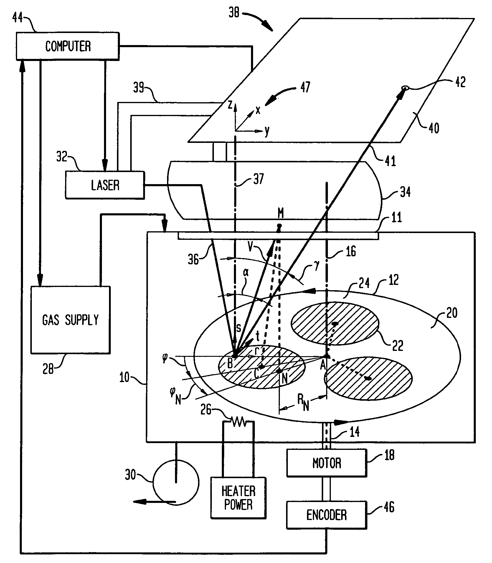
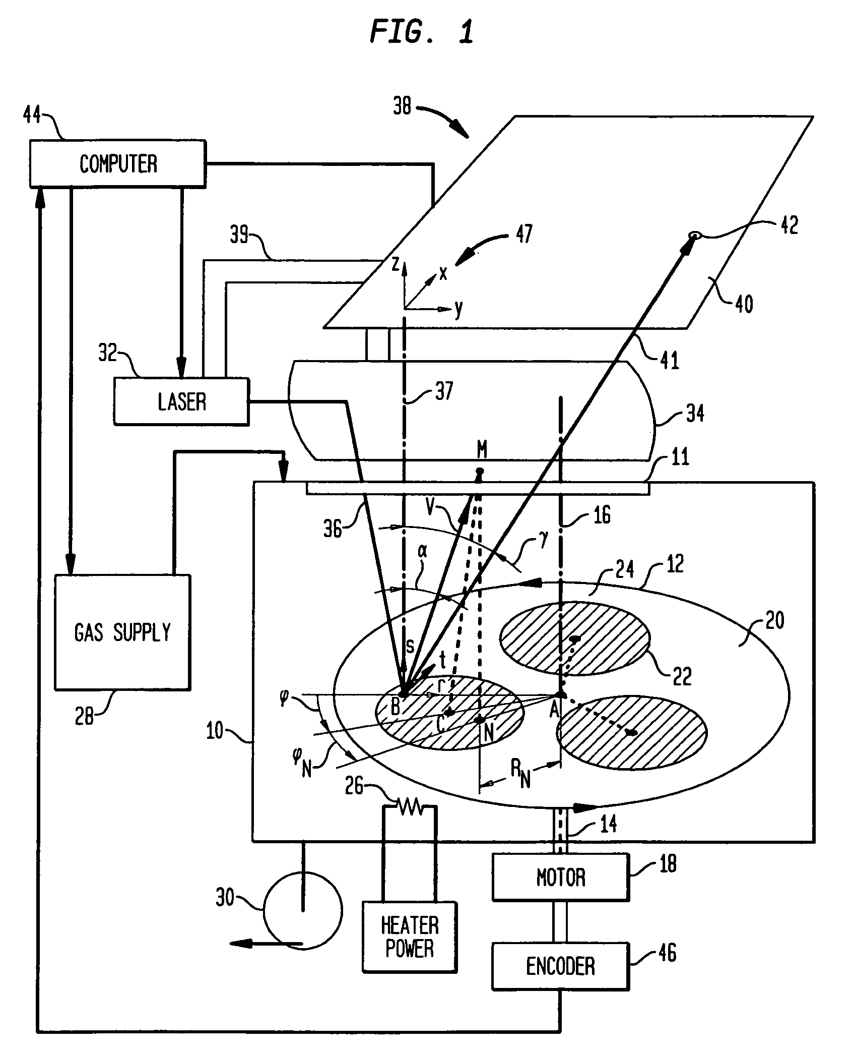
[0014]A system according to one embodiment of the present invention incorporates a structure having a chamber 10 and a disk-like carrier 12 mounted within chamber 10 on a shaft 14, so that the carrier 12 can be rotated about an axis of revolution 16, nominally perpendicular to the surface of the carrier. Chamber 10 has one or more optically transparent windows as, for example, a window 11 in the top wall of the chamber, above the carrier. The size of window 11 relative to chamber 10 is greatly exaggerated in FIG. 1 for clarity of illustration. A motor drive 18 is connected to shaft 14 for rotating the carrier. Carrier 12 has a front or top surface 20 with shallow pockets 22 formed therein. Each pocket is adapted to hold a disk-like wafer 24 so that a nominally planar major surface of the wafer faces upwardly (toward the top of the drawing in FIG. 1), and so that wafer is remote from the axis of revolution 16. A heater 26 is mounted within the chamber for maintaining the carrier at a...


PUM


Abstract

A method for monitoring the curvature of a surface of a body such as a semiconductor wafer (22) includes directing a beam of light along an impingement axis (36) onto the surface so that a beam of light (41) is reflected from the surface at a point of impingement. The position of the reflected beam (41) is detected in two dimensions (x,y). The body (22) is moved relative to the impingement axis (41) in a direction transverse to the impingement axis and the beam-directing and position determining steps are repeated. The curvature of the surface is calculated from the detected positions of the reflected beam in a plurality of repetitions.

Description

CROSS-REFERENCE TO RELATED APPLICATIONS[0001]The present application claims the benefit of the filing date of U.S. Provisional Patent Application No. 60 / 570,332 filed May 12, 2004 the disclosure of which is hereby incorporated by reference herein.BACKGROUND OF THE INVENTION[0002]The present invention relates to methods and apparatus for measuring the curvature of reflective surfaces such as the surfaces of semiconductor wafers.[0003]Semiconductors are commonly formed by epitaxial growth. In an epitaxial growth process, materials which form a layer, such as a semiconductor layer, are deposited onto the surface of a substrate, typically a crystalline substrate, so that the deposited material forms a generally crystalline structure having a crystal lattice similar to that of the substrate. The spacing between atoms within a crystal lattice (referred to as the “lattice spacing”) depends upon the composition of the crystal. Where the deposited layer has a composition different from the c...

Claims


Application Information

Patent Timeline
Patent Type & Authority Patents(United States)
IPC IPC(8): G01B11/24
CPCG01B11/24
Inventor BELOUSOV, MIKHAILVOLF, BORIS
Owner VEECO INSTR
Why Eureka
Try Eureka