Security application using silicon fingerprint identification

a fingerprint identification and security application technology, applied in the field of digital rights management, can solve the problems of cost or repeatability of chip identification values for cryptography, inability to measure values perfectly repeatable, and inability of hackers to discover secrets, etc., and achieve the effect of reducing the bit error rate of identification values

Inactive Publication Date: 2009-08-18
AVAGO TECH WIRELESS IP SINGAPORE PTE
View PDF2 Cites 23 Cited by
  • Summary
  • Abstract
  • Description
  • Claims
  • Application Information

AI Technical Summary

Benefits of technology

[0004]The present invention concerns a method for using an identification value for a security application. The method generally comprises the steps of (A) generating the identification value based on a plurality of semiconductor fabrication process variations, (B) generating a key by reducing a bit error rate of the identification value, wherein the key may not be available external to the security application and (C) generating an output signal by one of (i) encoding and (ii) decoding an input signal in response to said key.
[0005]The objects, features and advantages of the present invention include providing a silicon fingerprint identification for security applications that may (i) be non-clonable, (ii) be tamper-proof, (iii) provide a read-only unique identification, (iv) operate without programming steps, (v) operate without on-chip nonvolatile memory, (vi) operate without device-unique Flash images, (vii) be well suited for localized encryption and decryption, (viii) maintain a unique identification value totally within a chip and / or (ix) bury a root-of-trust inside the silicon.

Problems solved by technology

If the chip identification value were kept confined inside the packaged chip, and used only by internal chip resources, then efforts by hackers to discover the secret are greatly frustrated.
Problems with using chip identification values for cryptography are cost or repeatability.
Random identification values established during fabrication produce measured values that are not perfectly repeatable.

Method used


Image

  • Security application using silicon fingerprint identification
  • Security application using silicon fingerprint identification
  • Security application using silicon fingerprint identification

Examples


Embodiment Construction

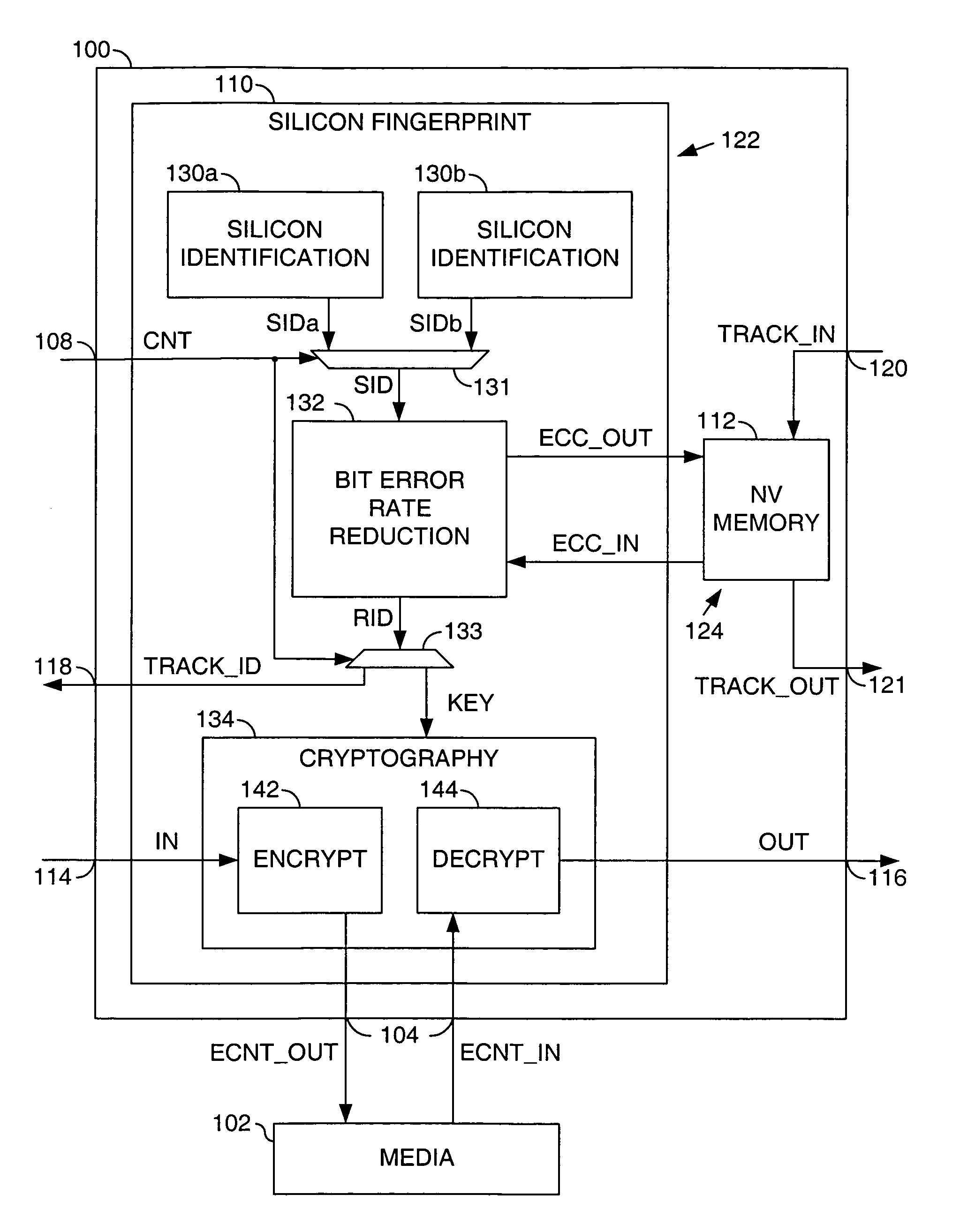
[0011]Referring to FIG. 1, a block diagram of circuit 100 is shown in accordance with a preferred embodiment of the present invention. The circuit (or system) 100 may be referred to as a identification (ID) circuit. The ID circuit 100 may communicate with a media 102 through an interface 104 for sending and / or receiving encrypted content. The ID circuit 100 may optionally receive a signal (e.g., CNT) through an interface 108 to command a presentation of a tracking identification value.

[0012]The ID circuit 100 generally comprises a circuit (or module) 110 and an optional circuit (or module) 112. In an encryption application, an input signal (e.g., IN) may be received at an input 114 by the circuit 110 and an output signal (e.g., ECNT_OUT) may be presented by the circuit 110 to the media 102. In a decryption application, an input signal (e.g., ECNT_IN) may be received from the media 102 and an output signal (e.g., OUT) may be presented from the circuit 110 at an output 116.

[0013]An op...


PUM


Abstract

A method for using an identification value for a security application is disclosed. The method may include the steps of (A) generating the identification value based on a plurality of semiconductor fabrication process variations, (B) generating a key by reducing a bit error rate of the identification value, wherein the key may not be available external to the security application and (C) generating an output signal by one of (i) encoding and (ii) decoding an input signal in response to said key.

Description

FIELD OF THE INVENTION[0001]The present invention relates to digital rights management generally and, more particularly, to security applications using a silicon fingerprint identification.BACKGROUND OF THE INVENTION[0002]An advantage for some security applications would be to keep a unique chip identification value a secret. If the chip identification value could be read from outside the packaged chip, then the secret would be exposed to hackers. If the chip identification value were kept confined inside the packaged chip, and used only by internal chip resources, then efforts by hackers to discover the secret are greatly frustrated. Furthermore, if each chip contains a statistically-unique identification value, no global secret (i.e., shared among devices of the same category) would exist to be discovered. The absence of a global secret greatly reduces a payoff of any hacking effort and thus should reduce an amount of effort a hacker would be willing to invest in mounting an attac...

Claims


Application Information

Patent Timeline
Patent Type & Authority Patents(United States)
IPC IPC(8): G06F11/30
CPCG06F21/10
Inventor BARR, DAVID A.
Owner AVAGO TECH WIRELESS IP SINGAPORE PTE
Why Eureka
Try Eureka